4 mcf5307 to s1d13705 interface, 1 hardware description – Epson S1D13705 User Manual
Page 489
Epson Research and Development
Page 13
Vancouver Design Center
Interfacing to the Motorola MCF5307 "ColdFire" Microprocessor
S1D13705
Issue Date: 01/02/13
X27A-G-011-02
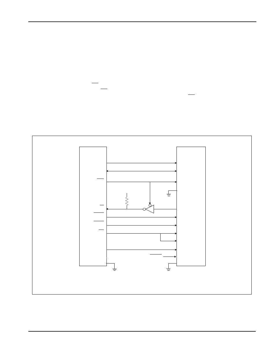
4 MCF5307 To S1D13705 Interface
4.1 Hardware Description
The S1D13705 is interfaced to the MCF5307 with a minimal amount of glue logic. One
inverter is required to change the polarity of the WAIT# signal, which is an active low
signal to insert wait states in the bus cycle, while the MCF5307’s Transfer Acknowledge
signal (TA) is an active low signal to end the current bus cycle. The inverter is enabled by
CS# so that TA is not driven by the S1D13705 during non-S1D13705 bus cycles. A single
resistor is used to speed up the rise time of the WAIT# (TA) signal when terminating the
bus cycle.
The following diagram shows a typical implementation of the MCF5307 to S1D13705
interface.
Figure 4-1: Typical Implementation of MCF5307 to S1D13705 Interface
MCF5307
S1D13705
A[16:0]
D[31:16]
CS4
TA
BWE1
BWE0
OE
BCLK0
AB[16:0]
DB[15:0]
CS#
WAIT#
WE1#
WE0#
RD/WR#
RD#
BUSCLK
RESET#
Vcc
470
BS#
System RESET
Note:
When connecting the S1D13705 RESET# pin, the system designer should be aware of all
conditions that may reset the S1D13705 (e.g. CPU reset can be asserted during wake-up
from power-down modes, or during debug states).