4 s1d13705 configuration – Epson S1D13705 User Manual
Page 377
Epson Research and Development
Page 17
Vancouver Design Center
Interfacing to the Toshiba MIPS TMPR3912 Microprocessor
S1D13705
Issue Date: 01/02/13
X27A-G-004-02
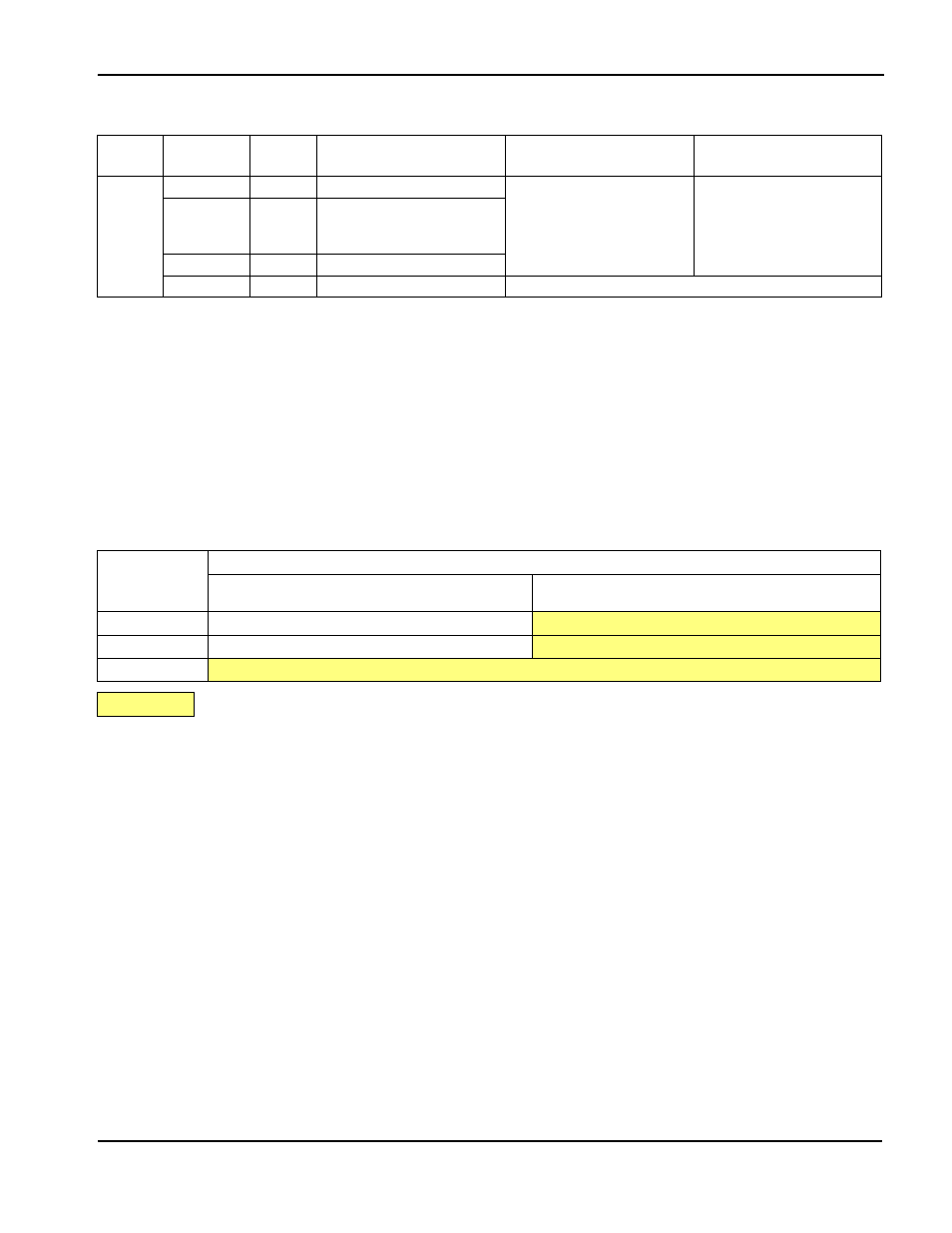
5.4 S1D13705 Configuration
The S1D13705 is configured at power up by latching the state of the CNF[3:0] pins. Pin
BS# also plays a role in host bus interface configuration. For details on configuration, refer
to the S1D13705 Hardware Functional Specification, document number X26A-A-001-xx.
The table below shows those configuration settings relevant to this specific interface.
2
0C00 0000h 16M byte
Card 2 IO
S1D13705
(aliased 512 times
at 128K byte intervals)
Card 2 IO
0D00 0000h 16M byte
S1D13705 (aliased 128
times
at 128K byte intervals)
0E00 0000h 32M byte
Card 2 Attribute
6800 0000h 64M byte
Card 2 Memory
S1D13705 (aliased 512 times at 128K byte intervals)
Table 5-2: S1D13705 Configuration Using the IT8368E
S1D13705
Configuration
Pin
Value hard wired on this pin is used to configure:
1 (IO V
DD
)
0 (V
SS
)
BS#
Generic #2
Generic #1
CNF3
Big Endian
Little Endian
CNF[2:0]
111: Generic #1 or #2
= configuration for connection using ITE IT8368E
Table 5-1: TMPR3912 to PC Card Slots Address Mapping With and Without the IT8368E
PC Card
Slot #
TMPR3912
Address
Size
Using the ITE IT8368E
Direct Connection,
CARDnIOEN=0
Direct Connection,
CARDnIOEN=1