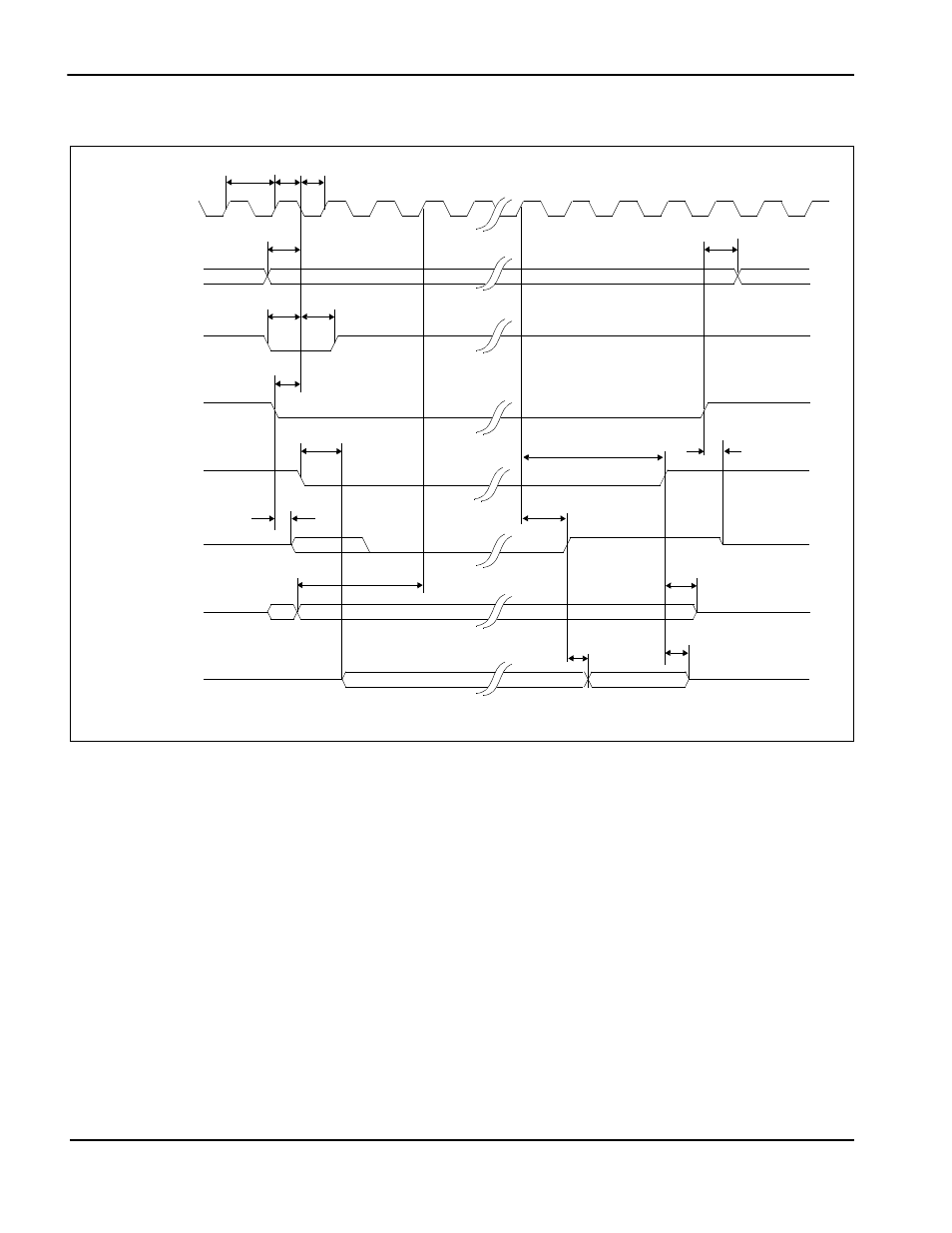
2 sh-3 interface timing, Figure 72: sh-3 bus timing, Sh-3 interface timing – Epson S1D13705 User Manual
Page 34: Figure 7-2: sh-3 bus timing

Page 28
Epson Research and Development
Vancouver Design Center
S1D13705
Hardware Functional Specification
X27A-A-001-10
Issue Date: 02/02/01
7.1.2 SH-3 Interface Timing
Figure 7-2: SH-3 Bus Timing
Note
The SH-3 Wait State Control Register for the area in which the S1D13705 resides must
be set to a non-zero value.
T
CKIO
t2 t3
t4
t11
t12
t16
t5
t6
t7
t8
t9
t13
t17
t14
t15
CKIO
A[16:0], M/R#
CSn#
RD/WR#
RD#
D[15:0]
BS#
WAIT#
WEn#
D[15:0]
Hi-Z
Hi-Z
Hi-Z
Hi-Z
Hi-Z
Hi-Z
VALID
(write)
(read)
t10
