4 vr4102/vr4111 to s1d13705 interface, 1 hardware description – Epson S1D13705 User Manual
Page 430
Page 12
Epson Research and Development
Vancouver Design Center
S1D13705
Interfacing to the NEC VR4102/VR4111 Microprocessor
X27A-G-008-02
Issue Date: 01/02/13
4 VR4102/VR4111 to S1D13705 Interface
4.1 Hardware Description
The NEC VR4102/VR4111 Microprocessor is specifically designed to support an external
LCD controller by providing the internal address decoding and control signals necessary.
By using the Generic # 2 interface, no glue logic is required to interface the S1D13705 and
the NEC VR4102/VR4111. A pull-up resistor is attached to WAIT# to speed up its rise time
when terminating a cycle.
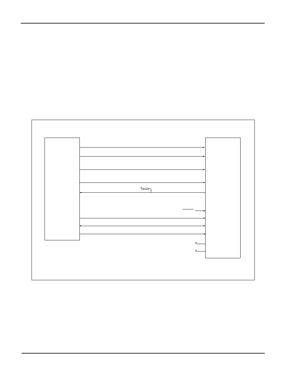
The following diagram shows a typical implementation of the VR4102/VR4111 to
S1D13705 interface.
Figure 4-1: Typical Implementation of VR4102/VR4111 to S1D13705 Interface
WE1#
WE0#
DB[15:0]
WAIT#
RD#
BUSCLK
S1D13705
CS#
RESET#
AB[16:0]
SHB#
WR#
DATA[15:0]
LCDCS#
RD#
BUSCLK
LCDRDY
ADD[16:0]
NEC VR4102/VR4111
Pull-up
BS#
RD/WR#
Vcc
Vcc
System RESET
Note:
When connecting the S1D13705 RESET# pin, the system designer should be aware of all
conditions that may reset the S1D13705 (e.g. CPU reset can be asserted during wake-up
from power-down modes, or during debug states).