Table 85: hardware power save/gpio0 operation, Table 86: software power save mode selection – Epson S1D13705 User Manual
Page 65
Epson Research and Development
Page 59
Vancouver Design Center
Hardware Functional Specification
S1D13705
Issue Date: 02/02/01
X27A-A-001-10
bit 3
LCDPWR Override
This bit is used to override the panel on/off sequencing logic. When this bit = 0, LCDPWR
and the panel interface signals are controlled by the sequencing logic. When this bit 1,
LCDPWR is forced to off and the panel interface signals are forced low immediately upon
entering power save mode. See Section 7.3.2, “Power Down/Up Timing” on page 37 for
further information.
bit 2
Hardware Power Save Enable
When this bit = 1 GPIO0 is used as the Hardware Power Save input pin. When this bit = 0,
GPIO0 operates normally.
bits 1-0
Software Power Save Bits [1: 0]
These bits select the Power Save Mode as shown in the following table.
Refer to Section 13, “Power Save Modes” on page 82 for a complete description of the
power save modes.
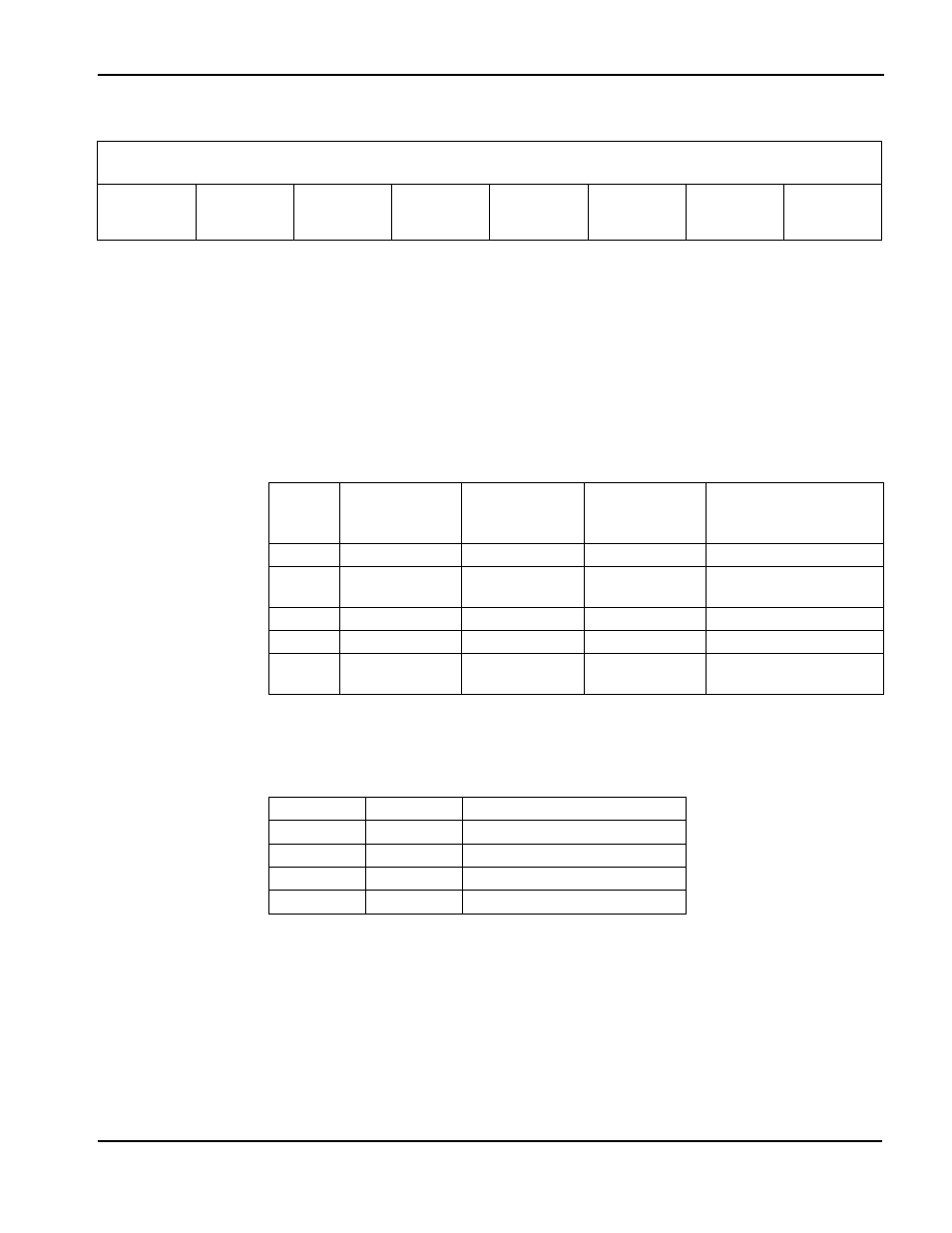
REG[03h] Mode Register 2
Address = 1FFE3h
Read/Write
n/a
n/a
n/a
n/a
LCDPWR
Override
Hardware
Power Save
Enable
Software
Power Save
Bit 1
Software
Power Save
Bit 0
Table 8-5: Hardware Power Save/GPIO0 Operation
RESET#
State
Hardware Power
Save Enable
REG[03h] bit 2
GPIO0 Config
REG[18h] bit 0
GPIO0
Status/Control
REG[19h] bit 0
GPIO0 Operation
0
X
X
X
1
0
0
reads pin status
GPIO0 Input
(high impedance)
1
0
1
0
GPIO0 Output = 0
1
0
1
1
GPIO0 Output = 1
1
1
X
X
Hardware Power Save
Input (active high)
Table 8-6: Software Power Save Mode Selection
Bit 1
Bit 0
Mode
0
0
Software Power Save
0
1
reserved
1
0
reserved
1
1
Normal Operation