Figure 21: mcf5307 memory read cycle, Figure 22: mcf5307 memory write cycle, 3 burst cycles – Epson S1D13705 User Manual
Page 485
Epson Research and Development
Page 9
Vancouver Design Center
Interfacing to the Motorola MCF5307 "ColdFire" Microprocessor
S1D13705
Issue Date: 01/02/13
X27A-G-011-02
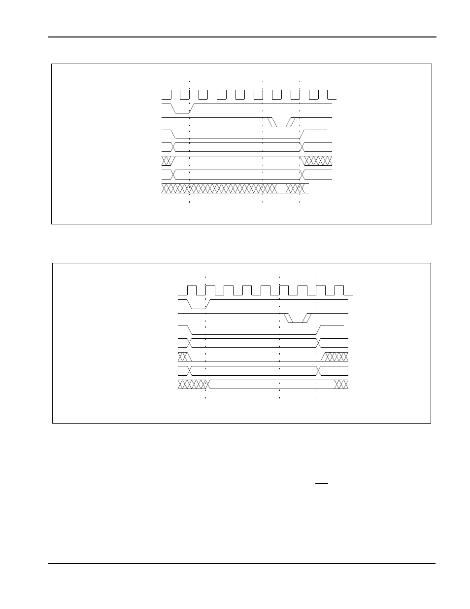
Figure 2-1: MCF5307 Memory Read Cycle
Figure 2-2: MCF5307 Memory Write Cycle
2.1.3 Burst Cycles
Burst cycles are very similar to normal cycles, except that they occur as a series of four
back-to-back, 32-bit memory reads or writes, with the TIP (Transfer In Progress) output
asserted continuously through the burst. Burst memory cycles are mainly intended to facil-
itate cache line fill from program or data memory; they are typically not used for transfers
to or from IO peripheral devices such as the S1D13705. The MCF5307 chip selects provide
a mechanism to disable burst accesses for peripheral devices which are not able to support
them.
A[31:0]
D[31:0]
SIZ[1:0], TT[1:0]
TS
TA
BCLK0
Wait States
Transfer Start
Transfer
Next Transfer
Sampled when TA low
R/W
Complete
Starts
TIP
A[31:0]
D[31:0]
SIZ[1:0], TT[1:0]
TS
TA
BCLK0
Wait States
Transfer Start
R/W
Valid
Transfer
Next Transfer
Complete
Starts
TIP