Table 42: cpu/bus connector (h2) pinout – Epson S1D13705 User Manual
Page 300
Page 12
Epson Research and Development
Vancouver Design Center
S1D13705
S5U13705B00C Rev. 1.0 ISA Bus Evaluation Board User Manual
X27A-G-005-03
Issue Date: 01/02/13
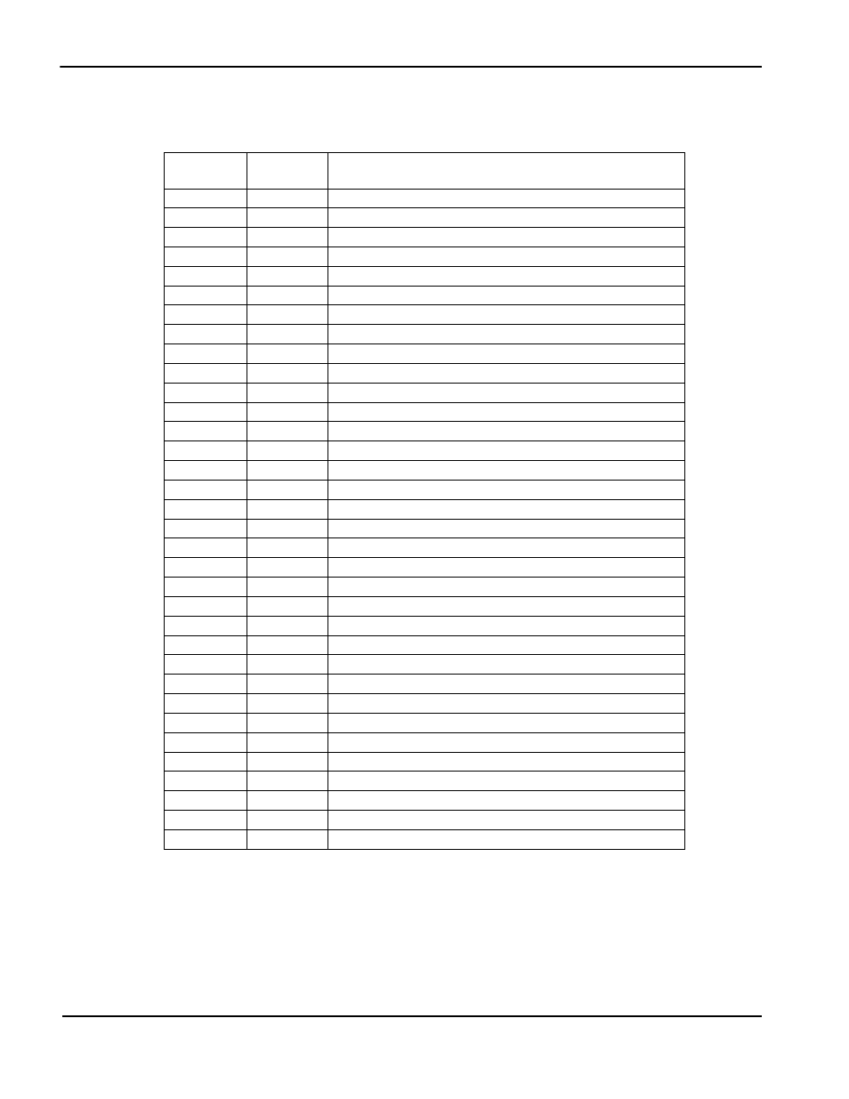
Table 4-2: CPU/BUS Connector (H2) Pinout
Connector
Pin No.
CPU/BUS
Pin Name
Comments
1
SA0
Connected to AB0 of the S1D13705
2
SA1
Connected to AB1 of the S1D13705
3
SA2
Connected to AB2 of the S1D13705
4
SA3
Connected to AB3 of the S1D13705
5
SA4
Connected to AB4 of the S1D13705
6
SA5
Connected to AB5 of the S1D13705
7
SA6
Connected to AB6 of the S1D13705
8
SA7
Connected to AB7 of the S1D13705
9
GND
Ground
10
GND
Ground
11
SA8
Connected to AB8 of the S1D13705
12
SA9
Connected to AB9 of the S1D13705
13
SA10
Connected to AB10 of the S1D13705
14
SA11
Connected to AB11 of the S1D13705
15
SA12
Connected to AB12 of the S1D13705
16
SA13
Connected to AB13 of the S1D13705
17
GND
Ground
18
GND
Ground
19
SA14
Connected to AB14 of the S1D13705
20
SA15
Connected to AB14 of the S1D13705
21
SA16
Connected to AB16 of the S1D13705
22
SA17
Connected to SA17 of the ISA bus connector
23
SA18
Connected to SA18 of the ISA bus connector
24
SA19
Connected to SA19 of the ISA bus connector
25
GND
Ground
26
GND
Ground
27
VCC
5 volt supply
28
VCC
5 volt supply
29
RD/WR#
Connected to the R/W# signal of the S1D13705
30
BS#
Connected to the BS# signal of the S1D13705
31
BUSCLK
Connected to the BCLK signal of the S1D13705
32
RD#
Connected to the RD# signal of the S1D13705
33
NC
Not connected
34
CLKI
Connected to the CLKI signal of the S1D13705