3 motorola mc68k #1 interface timing, Figure 73: mc68k #1 bus timing (mc68000), Table 73: mc68k #1 bus timing (mc68000) – Epson S1D13705 User Manual
Page 36: Motorola mc68k #1 interface timing, Table 7-3: mc68k #1 bus timing (mc68000), Figure 7-3: mc68k #1 bus timing (mc68000)
Page 30
Epson Research and Development
Vancouver Design Center
S1D13705
Hardware Functional Specification
X27A-A-001-10
Issue Date: 02/02/01
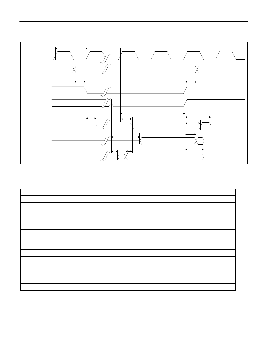
7.1.3 Motorola MC68K #1 Interface Timing
Figure 7-3: MC68K #1 Bus Timing (MC68000)
Note
CLK may be turned off (held low) between accesses - see Section 13.5, “Turning Off
BCLK Between Accesses” on page 84
Table 7-3: MC68K #1 Bus Timing (MC68000)
Symbol
Parameter
Min
Max
Units
f
CLK
Bus Clock Frequency
33
MHz
T
CLK
Bus Clock period
1/f
CLK
t1
A[16:1], CS# valid before AS# falling edge
0
ns
t2
A[16:1], CS# hold from AS# rising edge
0
ns
t3
AS# low to DTACK# driven high
16
ns
t4
CLK to DTACK# low
15
ns
t5
CLK to AS#, UDS#, LDS# high
1T
CLK
t6
AS# high to DTACK# high
20
ns
t7
AS# high to DTACK# high impedance
T
CLK
t8
UDS#, LDS# falling edge to D[15:0] valid (write cycle)
T
CLK
t9
D[15:0] hold from AS# rising edge (write cycle)
0
ns
t10
UDS#, LDS# falling edge to D[15:0] driven (read cycle)
15
ns
t11
D[15:0] valid to DTACK# falling edge (read cycle)
0
ns
t12
UDS#, LDS# rising edge to D[15:0] high impedance
10
ns
t3
A[16:1]
AS#
UDS#, LDS#
VALID
VALID
t1
t9
t2
t8
R/W#
Hi-Z
Hi-Z
INVALID
t6
t4
DTACK#
Hi-Z
Hi-Z
CLK
t7
T
CLK
CS#
t10
t11
Hi-Z
VALID
Hi-Z
D[15:0]
D[15:0]
t12
(write
(read)
t5