2 memory mapping and aliasing, 3 s1d13704/5 configuration and pin mapping – Epson S1D13705 User Manual
Page 525
EPSON Research and Development
Page 11
Vancouver Design Center
S5U13704/5 - TMPR3912/22U CPU Module
Issue Date: 01/03/07
X00A-G-004-02
3.2 Memory Mapping and Aliasing
The S1D13704 requires an addressing space of 64K bytes while the S1D13705 requires
128K. The on-chip display memory occupies the range 0 through 9FFFh. The registers
occupy the range FFE0h through FFFFh. The TMPR3912/22U demultiplexed address lines
A16 and above are ignored if the S1D13704 is used, thus it is aliased 1024 times at 64K
byte intervals over the 64M byte PC Card slot #1 memory space. If the S1D13705 is used,
address lines A17 and above are ignored; therefore the S1D13705 is aliased 512 times at
128K byte intervals. The TMPR3912/22U control signal CARDREG# is ignored; therefore
the S1D13704 also takes up the entire PC Card slot #1 configuration space.
Note
If aliasing is undesirable, additional decoding circuitry must be added.
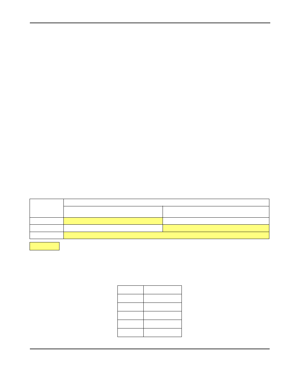
3.3 S1D13704/5 Configuration and Pin Mapping
The S1D13704/5 host bus interface is configured at power up by latching the state of the
CNF[3:0] pins. Pin BS# also plays a role in host bus interface configuration. One additional
configuration pin for the S1D13704, CNF4, is also used to set the polarity of the LCDPWR
signal.
The table below shows the configuration pin connections to configure the S1D13704/5 for
use with the TMPR3912/22U microprocessor.
When the S1D13704/5 is configured for Generic #2 bus interface mode, the host interface
pins are mapped as in the table below.
Table 3-1: S1D13704/5 Configuration for Generic #2 Bus Interface
S1D13704
Configuration
Pin
Value hard wired on this pin is used to configure:
1 (IO V
DD
)
0 (V
SS
)
BS#
Generic #2
Generic #1
CNF3
Big Endian
Little Endian
CNF[2:0]
111: Generic #1 or #2
= configuration for Toshiba TMPR3912/22U host bus interface
Table 3-2: S1D13704/5 Generic #2 Interface Pin Mapping
Pin Name
Pin Function
WE1#
BHE#
BS#
Connect to IO V
DD
RD/WR#
Connect to IO V
DD
RD#
RD#
WE0#
WE#