2 configuration jumpers, Table 32: jumper summary, Figure 32: configuration jumper (jp1) location – Epson S1D13705 User Manual
Page 323
Epson Research and Development
Page 11
Vancouver Design Center
S5U13705B00C Rev. 2.0 Evaluation Board User Manual
S1D13705
Issue Date: 2002/09/16
X27A-G-014-02
3.2 Configuration Jumpers
The S5U13705B00C has six jumper blocks which configure various setting on the board.
The jumper positions for each function are shown below.
JP1 - IOVDD Selection
JP1 selects the IOVDD voltage for S1D13705.
When the jumper is in position 1-2, IOVDD is 3.3V. This settings must be used for a 3.3V
host CPU system.
When the jumper is in position 2-3, IOVDD is 5.0V. This setting must be used for a 5.0V
host CPU system.
Note
For PCI host, JP1 can be set in either position.
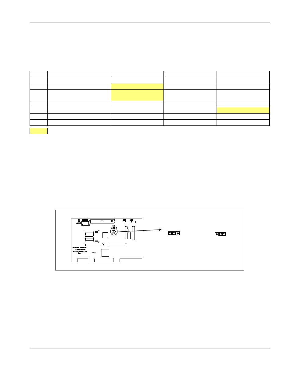
Figure 3-2: Configuration Jumper (JP1) Location
Table 3-2: Jumper Summary
Jumper
Function
Position 1-2
Position 2-3
No Jumper
JP1
IOVDD Selection
+3.3V IOVDD
+5.0V IOVDD
n/a
JP2
Bus Clock Selection
External Oscillator (U7)
From Host CPU
n/a
JP3
BS# Signal Selection
Pulled Down to GND (for
Generic #1 Interface)
Pulled High to IOVDD (for
Generic #2 Interface)
For SH-3, SH-4, MC68k #1
and MC68K #2 bus
JP4
LCD Panel Voltage Selection
+3.3V LCDVCC
+5.0V LCDVCC
n/a
JP5
PCI Bridge FPGA
Disabled for non-PCI host
n/a
Enabled for PCI host
JP6
LCDPWR Polarity
Active Low
Active High
n/a
JP7
CLKI Selection
External Oscillator (U2)
BCLK
n/a
= Required settings when used with PCI Bridge FPGA
JP1
3.3 Volt
5.0 Volt
IOVDD
IOVDD