4 mc68vz328 to s1d13705 interface, 1 hardware description, Using the mc68k #1 host bus interface – Epson S1D13705 User Manual
Page 412
Page 26
Epson Research and Development
Vancouver Design Center
S1D13705
Interfacing to the Motorola ‘Dragonball’ Family of Microprocessors
X27A-G-007-04
Issue Date: 01/02/13
4.4 MC68VZ328 To S1D13705 Interface
4.4.1 Hardware Description
The interface between the MC68VZ328 and the S1D13705 can be implemented using
either the MC68K #1 or Generic #1 host bus interface of the S1D13705.
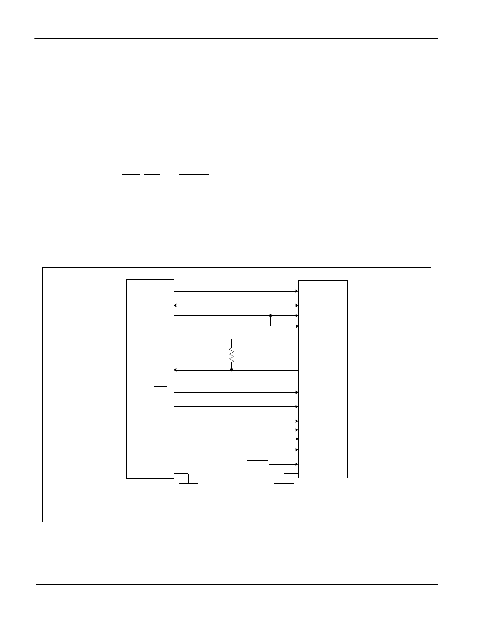
Using The MC68K #1 Host Bus Interface
The MC68VZ328 multiplexes dual functions on some of its bus control pins (specifically
UDS, LDS, and DTACK). In implementations where all of these pins are available for use
as bus control pins, then the S1D13705 interface is a straightforward implementation of the
“MC68K #1” host bus interface. Since AS is not provided by the DragonballVZ, CSB1 is
connected to BS# and indicates that a valid address is on the bus.
The following diagram shows a typical implementation of the MC68VZ328 to S1D13705
using the MC68K #1 host bus interface. For further information on the MC68K #1 host bus
interface and AC Timing, refer to the S1D13705 Hardware Functional Specification,
document number X27A-A-001-xx.
Figure 4-1: Typical Implementation of MC68VZ328 to S1D13705 Interface - MC68K #1
MC68VZ328
S1D13705
A[16:0]
D[15:0]
DTACK
UDS
LDS
R/W
CLK0
AB[16:1]
DB[15:0]
CS#
WAIT#
WE1#
AB0
RD/WR#
RD#
BUSCLK
RESET#
Vcc
1K
CSB1
BS#
Vcc
System RESET
WE0##
Vcc
Note:
When connecting the S1D13705 RESET# pin, the system designer should be aware of all
conditions that may reset the S1D13705 (e.g. CPU reset can be asserted during wake-up
from power-down modes, or during debug states).