Echelon Series 6000 Chip databook User Manual
Page 72

CP0
CP1
CP3
CP2
CP4
32 RX
34 TX
38
37 TXEN
39
Neuron 6000 Processor
LPT-11 Link Power
Transceiver
3.3 V Single-
Ended Mode
8
NETB
NETA
R1
10k
+3.3 V
+5 V
RXD
TXD
GND
VCC
INDUCTOR
6
9
10
4
5
NET_A
NET_B
2
1
GND
36
VDD3V3
Low drop-out
linear regulator
L1
1 mH
+5 V
+3.3 V
C4
0.1 pF
C3
22 µF
V+
3
C5
100 µF
OE
10 MHz
18 pF
C2
27 pF
C1
30 pF
R3
200
R2
1M
XOUT
XIN
CLK
7
+5 V
23
24
GROUND GUARD
U1
U2
U3
R4
10k
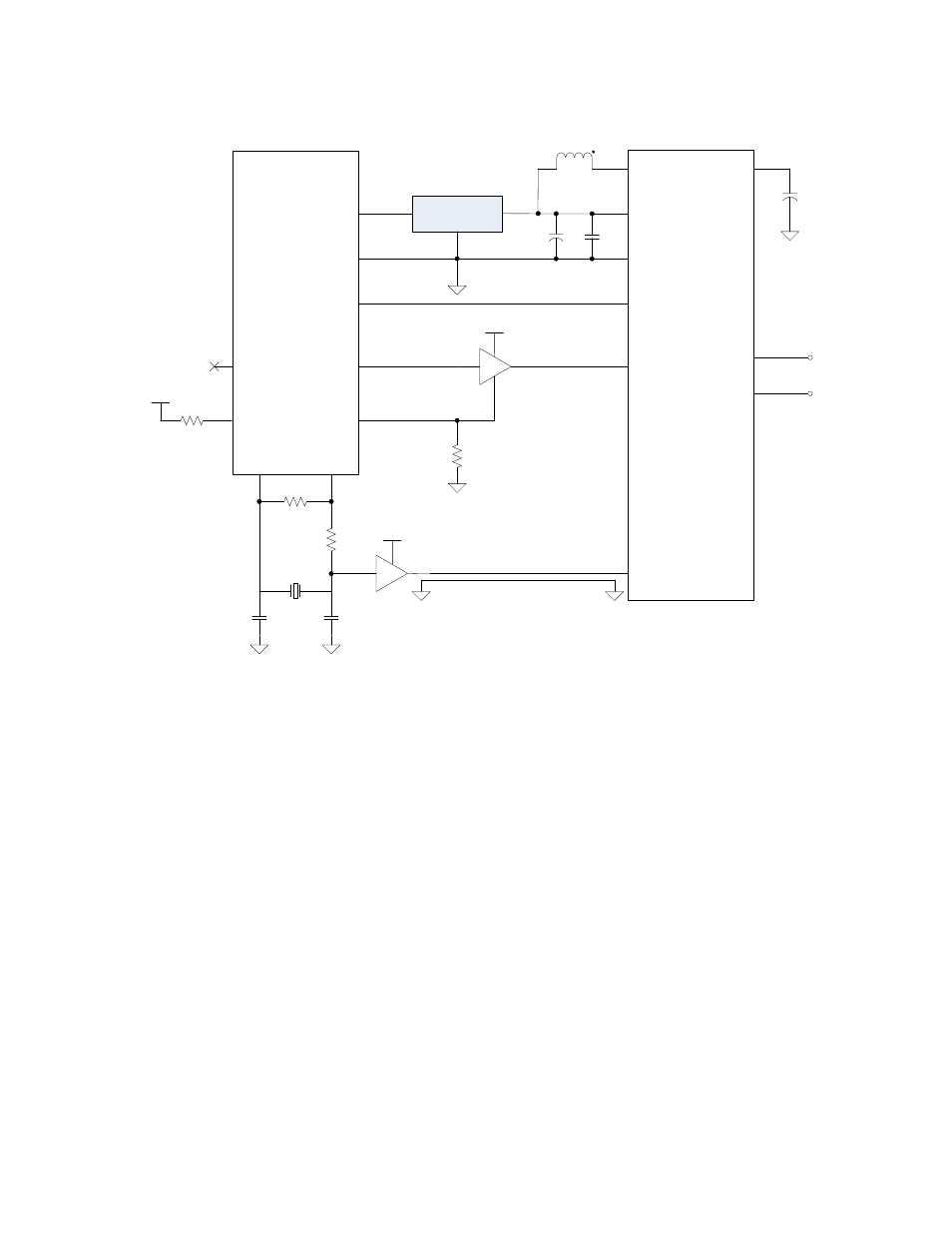
Figure 23. Connecting a Neuron 6000 Processor to an LPT-11 Link Power Transceiver
The major differences between connecting a Series 3100 Neuron Chip to an LPT-11
transceiver (see the L
ON
W
ORKS
LPT-11 Link Power Transceiver User’s Guide, 078-0198-01A)
and connecting a Neuron 6000 Processor to an LPT-11 transceiver are:
•
The connection between the LPT-11 VCC pin and the Neuron 6000 VDD3V3 pin
requires the addition of a low drop-out linear regulator to convert the +5 V output
from the LPT-11 transceiver to the +3.3 V input for the Neuron 6000 Processor.
•
The connection between the LPT-11 TXD pin and the Neuron 6000 CP1 pin requires
the addition of a non-inverting bus buffer/line driver that supports TTL-compatible
input and 5V CMOS output. The output of the Neuron CP2 pin is also connected to
the buffer/line driver to allow the Neuron 6000 Processor to propagate a device reset
to the LPT-11 transceiver by setting the buffer/line driver to a tri-state impedance
state. An example part for the buffer/line driver is an NXP
®
74AHCT1G126 bus
buffer/line driver.
•
The connection between the LPT-11 CLK pin and the Neuron 6000 XOUT pin
requires the addition of a standard (inverting or non-inverting) bus buffer/line driver
that supports TTL-compatible input and 5V CMOS output.
See the Connecting a Neuron 5000 Processor to an External Transceiver Engineering Bulletin
(005-0202-01B) for additional information.
60
Hardware Resources
