Electrostatic discharge design guidelines, Power supply, ground, and noise considerations – Echelon Series 6000 Chip databook User Manual
Page 157

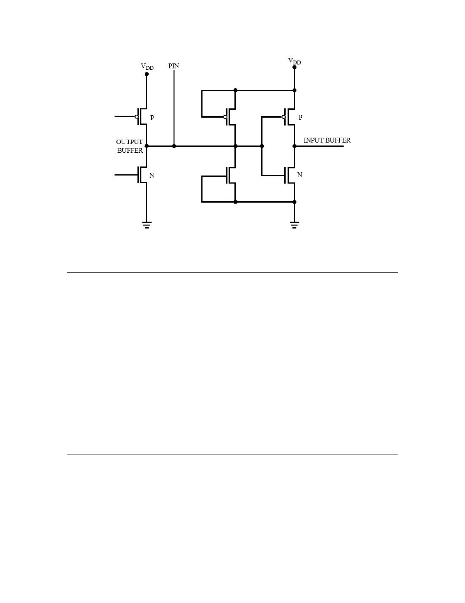
Figure 54. Digital I/O
Electrostatic Discharge Design Guidelines
There are many ways to deal with ESD, including:
•
Divert or limit energy from points of contact to circuitry.
•
Start with a series of electromagnetic interference (EMI) ferrites or resistors for high
frequency filtering.
•
Use diodes, transient voltage suppressors (such as, MOSorbs or transorbs) for high-
speed clamping.
•
Use capacitors to protect critical inputs.
•
Use good power distribution.
•
Use a separate, low-impedance, ESD ground path to divert energy from electronics
(for example, the star-ground strategy described in Chapter 4, Design and Test for
Electromagnetic Compatibility).
Note: The impedance of a wire at 300 MHz is approximately 20 Ω/cm. Use a conductor with
less than or equal to 3:1 length:width ratio.
Power Supply, Ground, and Noise Considerations
Some of the most important considerations for PCB layout concern how to manage noise.
Noise can come from the power supply, from digital circuitry on the device, and from digital
signals that couple to analog signals. Best practices for PCB layout methods to help prevent
noise-induced problems include:
•
Keep digital signals as far away from analog signals as possible.
Series 6000 Chip Data Book
145
