Transformer pad layout – Echelon Series 6000 Chip databook User Manual
Page 150

D3A
BAV99
1
3
BAV99
D4B
1
3
D3B
BAV99
3
2
BAV99
D4A
3
2
+
C6
22 uF
63V
1
2
+
C7
22 uF
63V
1
2
VR1
470V
1
2
JP1
HDR2 200 MIL R/A
2
1
NETB
NETA
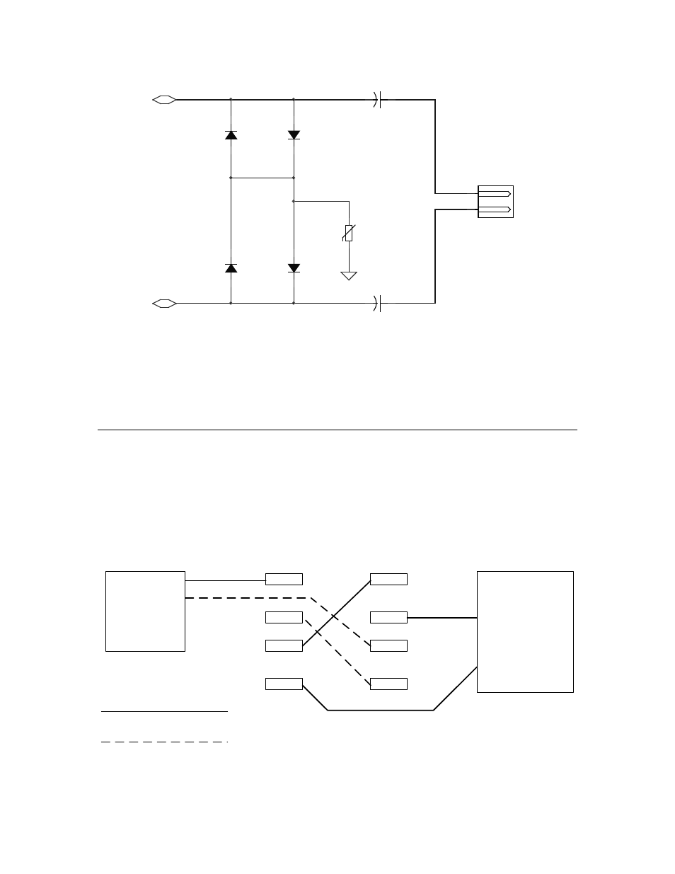
Figure 49. FT Network Electrical Connections
In the figure, the diodes D3 and D4 are differential network clamping diodes. Capacitors C6
and C7 are DC blocking capacitors, 22 µF, 63 V, polarized electrolytic aluminum. Varistor
VR1 is 470 V, 5 mm. See Connection for an FT 6000 Smart Transceiver for more information
about the network connection.
Transformer Pad Layout
See the FT 6000 Free Topology Smart Transceiver data sheet (for a description of the pad
layout for the FT-X3 Communications Transformer.
Figure 50 shows the recommended PCB trace layout for the FT-X3 Communications
Transformer for a two-layer PCB.
FT 6000
Smart
Transceiver,
C4-C5,
D1-D2
Network
Connection
and
C6-C7, VR1,
D3-D4
5
6
7
8
4
3
2
1
NETP
NETN
NETB
NETA
Bottom Side Traces
Top Side Traces
FT-X3 SMT
Pad Pattern (Top Side)
Figure 50. Recommended PCB Layout for FT-X3 Transformer
138
FT-X3 Communications Transformer
