Echelon Series 6000 Chip databook User Manual
Page 156

causes leakage or shorts. Often secondary damage occurs after an initial zap failure
causes a short.
•
Latch-up refers to a usually catastrophic condition that is caused by turning on a
parasitic, bipolar, silicon-controlled rectifier (SCR). A latch-up is formed by N and P
regions in the layout of the integrated circuit, which act as the collector, base, and
emitter of parasitic transistors. Bulk resistance of silicon in the wells and substrate
acts as resistors in the SCR circuit. Application of voltages to pins above V
DD
+ 0.3 V
or below GND – 0.3 V, in conjunction with enough current to develop voltage drops
across the parasitic resistors, can cause the SCR to turn on. After it is on, the SCR
can be turned off only by removal of all power and applied voltages. The low on-
impedance of the SCR circuit can overheat and destroy the chip.
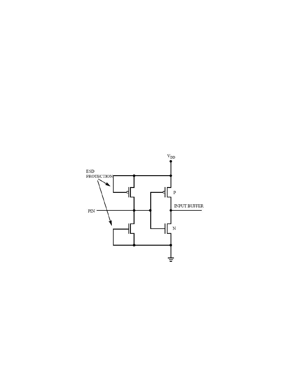
Figure 53 shows the MOS circuitry for a digital input-only pin. The gates of the input buffer
are very high impedance for all voltages that would ever be applied to the pin. Protection is
implemented with a P-channel transistor that acts as a diode to V
DD
and an N-channel
transistor that acts as a diode to GND. Allowing a pin to float or be driven to a mid-supply
level can result in both the N- and P-channel devices in the input buffer simultaneously
being partially on, which can cause excess current and noise for the V
DD
/GND power supply.
If a digital input is driven above V
DD
, the pseudo-diode will conduct, protecting the input. As
the current is increased to high levels (100 mA), damage can result.
Figure 53. Digital Input
Figure 54 shows the CMOS circuitry for a digital I/O pin.
144
Handling and Manufacturing Guidelines
