Echelon Series 6000 Chip databook User Manual
Page 52

FT 6000
Smart Transceiver
U1
FT 5000
SVC~
1
IO0
2
IO1
3
IO2
4
IO3
5
VDD1V8
6
IO4
7
VDD3V3
8
IO5
9
IO6
10
IO7
11
IO8
12
IO
9
13
IO
10
14
IO
11
15
VDD
1
V
8
16
TRST
~
17
VDD
3
V
3
18
TCK
19
TMS
20
TDI
21
TDO
22
XIN
23
XOUT
24
VDDPLL
25
GNDPLL
26
VOUT1V8
27
RST~
28
VIN3V3
29
VDD3V3
30
AVDD3V3
31
NETN
32
AGND
33
NETP
34
NC
35
GND
36
TXON
37
RXON
38
CP
4
39
CS
0
~
40
VDD
3
V
3
41
VDD
3
V
3
42
SDA
_
CS
1
~
43
VDD
1
V
8
44
SCL
45
MISO
46
SCK
47
MOSI
48
GND
49
VDD33
VDD33
C2
0.1 uF
1
2
C1
0.1 uF
1
2
C4
0.1 uF
1
2
C3
0.1 uF
1
2
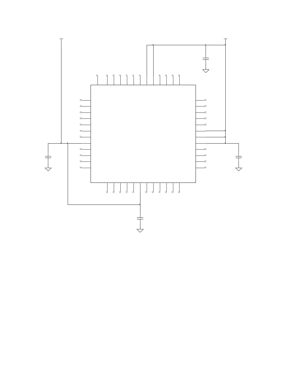
Figure 10. Connections for the VDD33 Pins
In the figure, the capacitors are:
•
C1-C4: 0.1 µF Ceramic
The VOUT1V8 pin (27) is the output of the on-chip voltage regulator. Connect the VDD1V8
pins (6, 16, and 44) to the VOUT1V8 pin (27) to connect the 1.8 V input pins to the output of
the internal voltage regulator, as shown in Figure 11. Connect a bulk decoupling capacitor
(C5 in Figure 11) near the VOUT1V8 pin (27), in addition to the other decoupling capacitor.
Important: Do not connect an external 1.8 V source to any of the VDD1V8 pins (6, 16, and
44). Connect these pins to the VOUT1V8 pin (27) only. Using an external 1.8 V source
voids the warranty for the chip, and can cause unpredictable and possibly
irreparable results.
40
Hardware Resources
