Transformer pinout – Echelon Series 6000 Chip databook User Manual
Page 148

Transformer Pinout
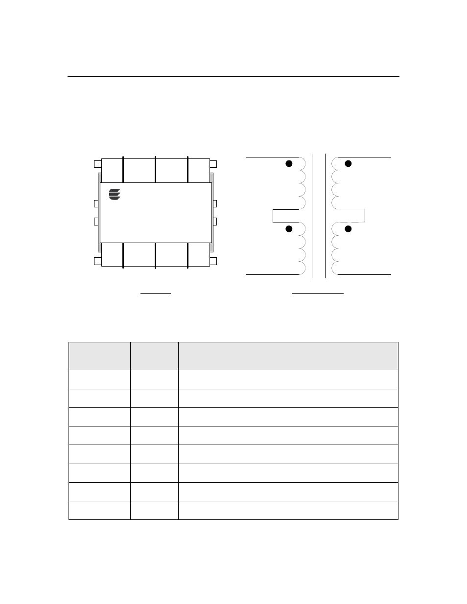
Figure 49 shows the pinout for the FT-X3 Communications Transformer and the equivalent
electrical schematic. The FT-X3 Communications Transformer is rotationally symmetric;
thus, the package does not mark pin 1. The wiring connections shown in Figure 47 are made
on the PCB, as described in Transformer Pad Layout. Table 42 lists the pin assignments for
the FT-X3 Communications Transformer.
Winding
P1
Winding
S2
Winding
P2
Winding
S1
n
n
n
n
1
2
5
6
3
8
7
4
Top View
Pin 1
Pin 2
Pin 3
Pin 4
Pin 5
Pin 6
Pin 7
Pin 8
FT-X3
®
Schematic View
Figure 47. FT-X3 Communications Transformer Pinout Diagram and Schematic
Table 42. FT-X3 Communications Transformer Pin Assignments
Name
Pin
Number
Description
NETP
1
NETP connection from FT 6000 Smart Transceiver
CTP1
2
Center tap for primary winding 1
CTS2
3
Center tap for secondary winding 2
NETA
4
NETA connection to L
ON
W
ORKS
network
CTP2
5
Center tap for primary winding 2
NETN
6
NETN connection from FT 6000 Smart Transceiver
NETB
7
NETB connection to L
ON
W
ORKS
network
CTS1
8
Center tap for secondary winding 1
136
FT-X3 Communications Transformer
