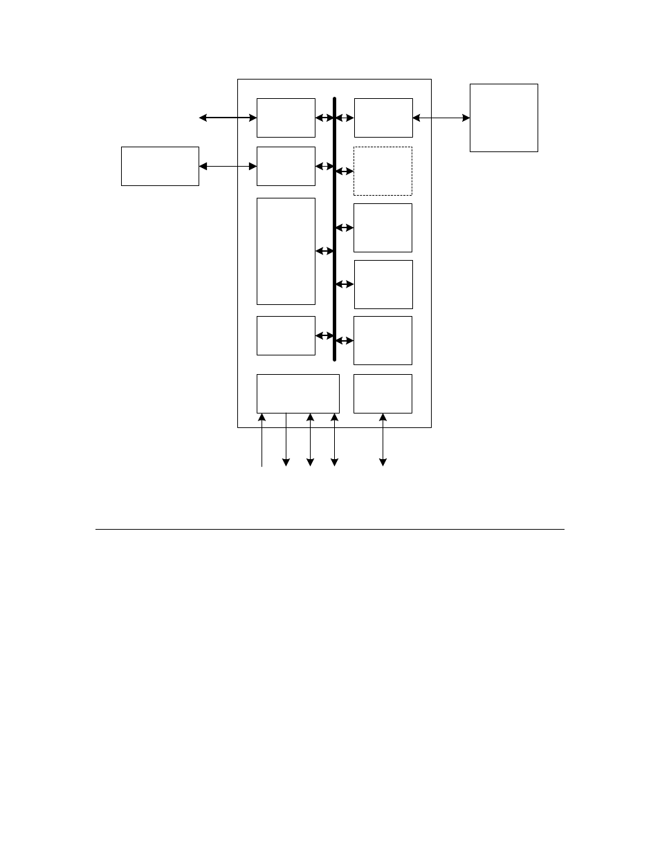
Neuron processor architecture, Figure 3 – Echelon Series 6000 Chip databook User Manual
Page 27

Clock, Reset,
and Service
Serial
Memory
Interface
RAM
(64K x 8)
I/O
Comm
Port
NET CPU
Transformer
or
transceiver
NVM
(SPI)
ROM
(16K x 8)
JTAG
APP CPU
IRQ CPU
MAC
CPU
XIN
XOUT
RST
~
/
/
/
/
12
5
5
6
SVC
~
Figure 3. Series 6000 Chip Architecture
Neuron Processor Architecture
The basic Neuron processor architecture is stack-oriented:
•
An 8-bit-wide stack is used for data references, and the arithmetic-logic unit (ALU)
operates on the TOS (Top of Stack) register and on the next entry in the data stack
(which is in RAM).
•
Another stack stores the return addresses for CALL instructions, and can also be
used for temporary data storage.
This stack architecture leads to very compact code. See Assembly Instruction Set for a
summary of the instruction set.
Figure 4 shows the layout of a base page, which can be up to 256 bytes long. Each of the
chip’s processors uses a different base page, whose address is given by the contents of the BP
(Base Page) register of that processor. The top of the data stack is in the 8-bit TOS register,
and the next element in the data stack is at the location within the base page at the offset
given by the contents of the DSP (Data Stack Pointer) register. The assembler shorthand
Series 6000 Chip Data Book
15
