Power distribution and decoupling capacitors, Recommended bypass capacitor placement – Echelon Series 6000 Chip databook User Manual
Page 163

7. Equipment specifications should alert users to the presence of CMOS devices and
require familiarization with this specification prior to performing any kind of
maintenance or replacement of devices or modules.
8. Do not insert or remove CMOS devices from test sockets with power applied. Check
all power supplies to be used for testing devices to be certain there are no voltage
transients present.
9. Double-check the equipment setup for proper polarity of voltage before conducting
parametric or functional testing.
10. Do not recycle shipping rails. Continuous use causes deterioration of their antistatic
coating.
11. Wrist straps and equipment logs should be maintained and audited on a regular
basis. Wrist straps malfunction and the malfunction can go unnoticed. Also,
equipment gets moved from time to time and grounds might not be reconnected
properly.
Power Distribution and Decoupling Capacitors
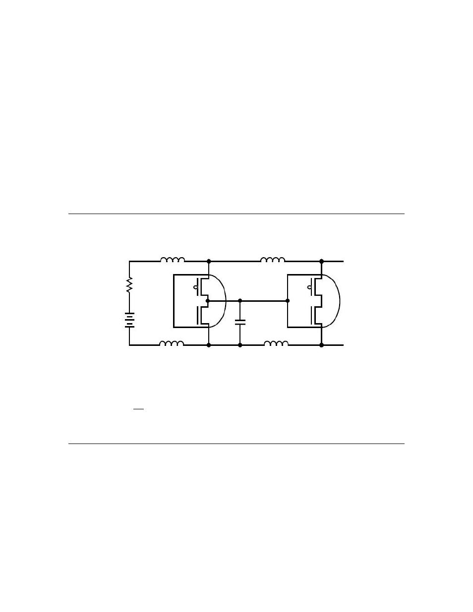
Inductance in the power distribution creates noise during switching transients.
Figure 57. Inductance Creates Noise
For example, a 200 nH inductor with 25 mA and 5 ns surge characteristic can generate 1 V
in noise:
dt
dI
L
V
noise
=
If L = 200 nH, dI = 25 mA, dt = 5 ns, then V
noise
= 200 nH * (25 mA / 5 ns) = 1 V.
Recommended Bypass Capacitor Placement
Proper decoupling is required to ensure proper operation of an FT 6000 Smart Transceiver or
Neuron 6000 Processor. When you connect V
DD
decoupling capacitors to Series 6000 chips,
make the leads as short as possible. All V
DD
pins must be tied to +3.3 V, and all GND pins to
ground. Keep the crystal circuit close to the Series 6000 chip and isolated from
communications lines.
Bypass capacitors should be 0.1 μF or 0.33 μF ceramic or dipped-mica capacitors, and should
be placed as close to V
DD33
pins as possible. V
DD33
and GND loops should be avoided.
Recommended configurations are:
Series 6000 Chip Data Book
151
