Characteristics of the digital pins, Characteristics of the digital pins ) – Echelon Series 6000 Chip databook User Manual
Page 55

VDD3
R1
4.99k
1
2
TCK
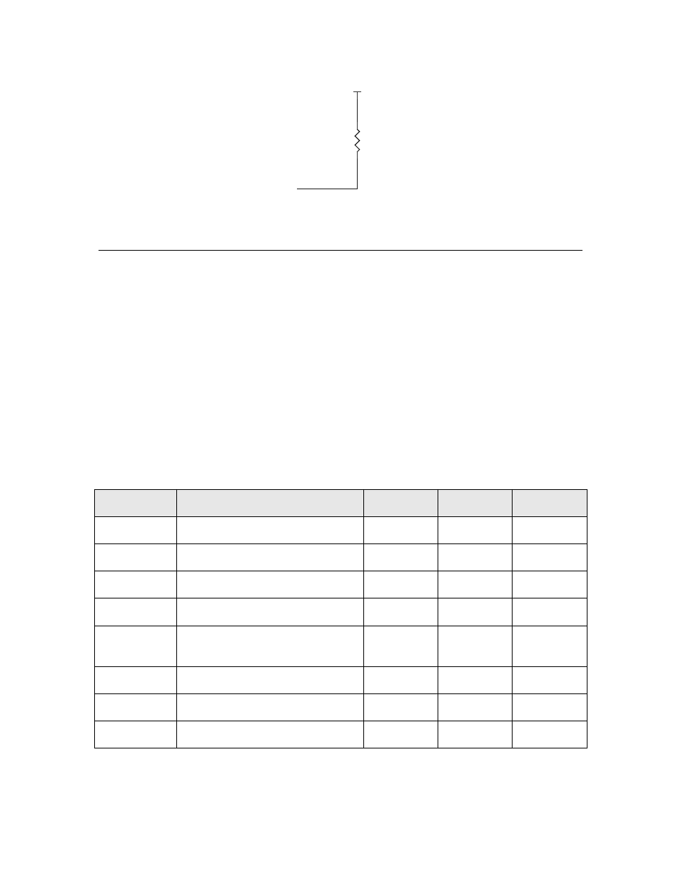
Figure 14. Connection for the JTAG TCK Pin
Characteristics of the Digital Pins
Series 6000 chips provide 12 bidirectional I/O pins that are usable in several different
configurations. These pins provide flexible interfacing to external hardware and access to
the internal timer/counters. In addition to reading the input pins, the application processor
can read the current logic level of the output pins.
The digital I/O pins (IO0 – IO11) have LVTTL-level inputs. Pins IO0 – IO7 also have low-
level-detect latches. The RST~ and SVC~ pins have internal pull-ups, and the RST~ pin
has hysteresis.
See the I/O Model Reference for Smart Transceivers and Neuron Chips for more information
about how to use the digital I/O pins.
Table 16 lists the characteristics of the digital I/O pins, which include the IO0 – IO11 pins,
the memory I/O pins, the Neuron 6000 CP0 – CP4 pins, and the other digital pins listed in
Table 16. Series 6000 Chip Digital Pin Characteristics
Parameter
Description
Minimum
Typical
Maximum
V
OH
Output drive high at I
OH
= 8 mA
2.4 V
—
V
DD3
V
OL
Output drive low at I
OL
= 8 mA
GND
—
0.4 V
V
IH
Input high level
2.0 V
—
5.5 V
V
IL
Input low level
GND
—
0.8 V
V
HYS
Input hysteresis for RST~ pin
and TCK pin
—
300 mV
—
I
IN
Input leakage current
—
—
10 µA
R
PU
Pullup resistance
13 kΩ
—
23 kΩ
I
PU
Pullup current when pin at 0 V
—
275 µA
Series 6000 Chip Data Book
43
