Sensor amplifier, Sensor amplifier -3 – KEYENCE IG Series User Manual
Page 115
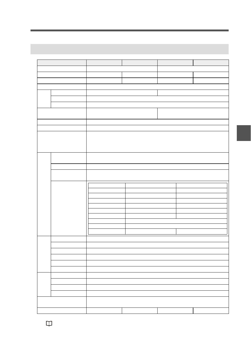
5-1 Specifications
5-3
IG-E
5
Specific
a
tion
s
*1 When expansion units are added: 20 mA/ch
*2
"3. Average number of times (Response time)" (page 4-17)
*3 Delay time that occurs from the analog output circuit after the judgment is output.
*4 For detailed time chart, refer to "11. External input" (page 4-33).
Sensor Amplifier
Model
IG-1000
IG-1050
IG-1500
IG-1550
Type
DIN rail mount
Panel mount
Main unit/Expansion unit
Main unit
Expansion unit
Main unit
Expansion unit
Analog output
Yes
No
Yes
No
Power supply voltage
DC10-30V Ripple (P-P) 10 % included
Power
consump-
tion
Normal
2700 mW or less (at 30 V:90 mA or less) 2880 mW or less (at 30 V:96 mA or less)
Power save function:Half
2300 mW or less (at 30 V: 77 mA or less)
Power save function:Full
2200 mW or less (at 30 V: 74 mA or less)
Digital display method
Dual 7-seg display
Upper level: Red, 5 digits, Lower level: Green, 5 digits
Dual 7-seg display
Upper level: Red/Green, 2 colors, 5 digits, Lower level: Green, 5 digits
Display range
-99.999 to 99.999, -99.99 to 99.99, -99.9 to 99.9, -99 to 99 (selectable)
Display resolution
1
P
m, 10
P
m, 100
P
m, 1000
P
m (selectable)
Operation status
indicator
Judgment indicator: Red/Green 2 colors LED (HI, LO, GO)
Bank indicator: Green LED x 4
Laser emission indicator: Green LED
Others: Green LED x 8, Red LED x 3
Out-
put
Judgment output
(selectable between NPN and PNP)
NPN (PNP) Open collector x 3 ch, DC 30 V (Power supply voltage) or less,
Residual voltage 1 V (2 V) or less, NO/NC selectable, Max. 50 mA/ch
*1
Response time (judgment output)
1.96 to 4031.72 ms
*2
Edge check output
(selectable between NPN and PNP)
NPN (PNP) Open collector x 1 ch, DC 30 V (Power supply voltage),
Residual voltage 1 V (2 V) or less, NO/NC selectable, Max. 50 mA
*1
, Response time 20 ms
Analog output
(selectable
among ±5 V,
1-5 V, 0-5 V,
4-20 mA)
Input
Gain input
Input time: 20 ms or more, Response delay time: 120 ms or less (When saving on nonvolatile memory (EEPROM): 1.5 s)
Reset input
Input time: 20 ms or more, Response delay time: 20 ms or less
Timing Input
Input time: 2 ms or more, Response delay time: 2 ms or less
Zero shift input
Input time: 20 ms or more, Response delay time: 20 ms or less
Bank A input/Bank B input
Input time: 20 ms or more, Response delay time: 20 ms or less
*4
Laser emission stop input
Input time: 2 ms or more, Response delay time: 2 ms or less
Environ-
ment
resis-
tance
Ambient temperature
-10 to +50 °C (No freezing)
Ambient humidity
35 to 85% RH (No condensation)
Vibration resistance
10 to 55 Hz Double amplitude 1.5 mm X, Y, Z each axis: 2 hours
Pollution degree
2
Material
Main unit case/Front sheet: Polycarbonate,
Key top: Polyacetal, Cable: PVC
Weight (including supplied items)
Approx. 150 g
Approx. 140 g
Approx. 170 g
Approx. 165 g
Voltage output
Current output
Output range
±5 V (full scale 10 V)
4-20 mA (full scale 16 mA)
Output resistance
100
:
-
Maximum load resistance
-
350
:
Repetition accuracy
±1mV
±1.5
P
A
Display accuracy
±0.05 % of F.S.
±0.25 % of F.S.
Temperature characteristics
±0.005 % of F.S./°C
±0.01 % of F.S./°C
Update cycle
Same as sensor head sampling cycle
Response delay time
Same as Response time (judgment output)
Time constant
*3
10
P
s (90 % response)
30
P
s (90 % response)