Elecraft K2 Owner's Manual User Manual
Page 39
38
E
LECRAFT
®
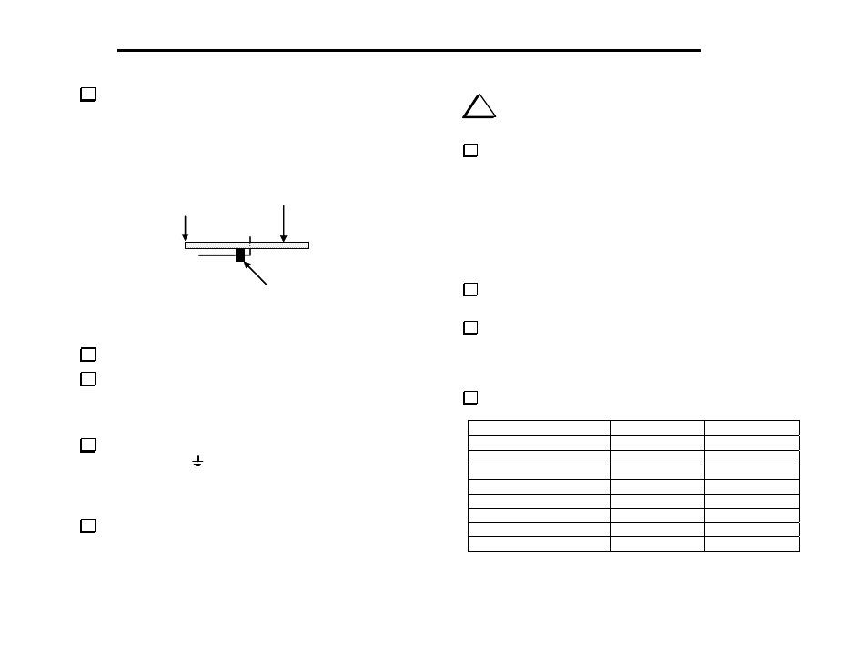
Position 20-pin male right-angle connector P1 on the bottom of
the board (Figure 6-5), but do not solder P1 yet. Review Figure 3-3
(page 8) for correct placement. The short ends of the bent pins are
inserted into the holes, and the long ends must be parallel with the
board.
Front edge
P1
Top of board
Figure 6-5
Solder just the two end pins of P1.
Look closely at P1 to make sure that its plastic support is pressed
down as far as it will go, and that the pins are parallel to the board. If
not, re-heat the soldered ends while pressing it into place. Once it is
seated properly, solder the remaining pins.
To the left and right of the I/O controller, U1, you’ll find two
short jumpers labeled "
" or "GND" (on the top side of the board).
Form 3/4" (19 mm) long U-shaped ground jumpers and install them at
these locations as you did on the control and Front Panel boards. Use
discarded component leads.
On the bottom of the board you’ll find two additional ground
jumpers, one near the middle and the other near the back edge. Install
U-shaped ground jumpers in these two locations.
i
Before handling U1, touch an unpainted, grounded metal
surface or put on a conductive wrist-strap.
Install the I/O controller, U1 (PIC16F872 or 16F872A), in its
socket (near the middle of the board). Be sure to align the notched or
dimpled end of U1 with the notched end of the socked (to the left).
Make sure U1 is seated as far down in the socket as it will go and that
none of its pins are bent. Note: The revision label on U1 may not be
oriented in the same direction as the text printed on the IC. Use only
the notch or dimple to identify the pin 1 end.
Visual Inspection
Examine the RF board carefully for unsoldered pins, solder
bridges, or cold solder joints.
Set switch S1 on the RF board to the "OFF" position. (Plunger
OUT is OFF, plunger IN is ON.)
Resistance Checks
Perform the following resistance checks.
Test Point
Signal Name
Res. (to GND)
R115, right end (near S1)
12V IN
> 500 ohms
U1 pin 1
6V
> 500 ohms
U1 pin 4
K13 control
> 20 k
U1 pin 9
OSC1
> 20 k
U1 pin 10
OSC2
> 20 k
U1 pin 28
AUXBUS
> 20 k
R1 (end near R2)
DOT/PTT
> 1 M
R2 (end near R1)
DASH
> 1 M