Receiver and synthesizer – Elecraft K2 Owner's Manual User Manual
Page 162

10
T-R Switch
Band-Pass XMTR Low-pass
Filters Filters
U1 (I/O Controller)
Synthesizer RCVR
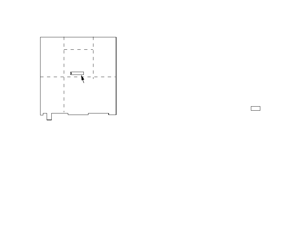
Figure 3
Receiver and Synthesizer
In the following steps you’ll use the RF probe and other techniques to find the
stage where the received signal is getting attenuated. (Figure 3 shows the
approximate location of the synthesizer, receiver, and other circuits on the RF
board.) You can then use voltage tables, resistance checks and close
examination to find the bad component or connection.
Perform all measurements in the order listed. In general, your measurements
can vary 20-25% from those shown and still be acceptable. Space is provided
to record your own measurements (in pencil), which will be very useful if you
need to re-test a particular circuit after repairs.
Preparation for Receiver Signal Tracing
1. Verify that basic display and control circuits are functioning.
2. Using your DMM, check the 5-V and 8-V regulator outputs.
3. Measure the voltages on the anodes (right end) of D6 and D7 (on the RF
board, near the I/O controller, U1). In receive mode, D6’s anode should
be at about 8 V, and D7’s should be near 0 V.
4. Connect the RF probe’s output to your DMM’s +/- DC input jacks.
5. Select a 2 or 3-V DC range.
6. The DMM should read close to 0.000 V DC. The reading should increase
when you touch the RF probe tip with your finger.
7. Turn on the K2 and switch to 30 m (or the appropriate band for your
signal generator). Select CW Normal mode.
8. Using the menu, select
O P T P E R F
.
9. Use
CAL FIL
to set up CW normal filter FL1 for a bandwidth of
1 . 50
. If you can hear some noise on your receiver, set up the BFO for
this filter as described in the Operation section of the manual. Otherwise,
set the BFO to the factory default value.
10. Exit
CAL FIL
, then select the 1.50-bandwidth filter using
X F I L
.
PLL Reference Oscillator and VCO (RF board schematic, sheet 1)
1. Connect the RF probe’s ground clip to the ground jumper near the
synthesizer circuitry.
2. Reference Oscillator Output: Measure the reference oscillator signal at
pin 1 of U4 (MC145170), which is near the front-left corner of the RF
board (near the control board). Expected: 0.8-1.8 Vrms. Actual: ______.
3. VCO Output: Measure the VCO signal at pin 3 of U3 (LT1252).
Expected: 0.30-0.40 Vrms. Actual: ______. If this signal is zero, you
may have the secondary winding of T5 reversed.
4. VCO Buffer Output: Measure the signal on pin 6 of U3. Expected:
0.60-0.75Vrms. Actual: ______.
5. Check the VCO frequency (RF Board, Alignment and Test Part II).
