Lenze EVF9383 User Manual
Page 115
Wiring of digital frequency input / digital frequency output
5.9
l
5.9−1
EDSVF9383V EN 7.1−04/2012
5.9
Wiring of digital frequency input / digital frequency output
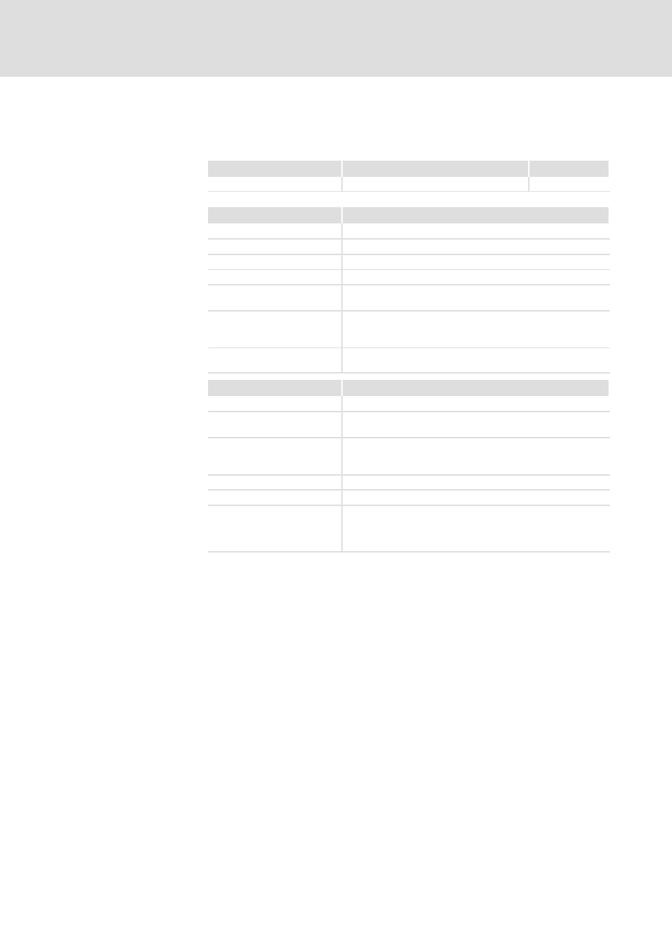
Installation material required from the scope of supply:
Description
Use
Quantity
Protective cover
Protection for unused Sub−D connections
4
Field
Digital frequency output X10
Connection at drive controller Connector: female, 9−pole, Sub−D
Pin assignment
Dependent on the selected basic configuration
Output frequency
0 ... 500 kHz
Signal
Two−track with inverse 5 V signals (RS422) and zero track
Load capacity
Max. 20 mA per channel
(up to 3 slave drives can be connected)
Special features
The "Enable" output signal at X10/8 switches to LOW if the
drive controller is not ready for operation (e.g. disconnected
from mains). This may trip SD3 monitoring on the slave drive.
Internal voltage source
(X10/4, X10/5)
DC 5 V / max. 50 mA
Total current at X9/4, X9/5 and X10/4, X10/5: max. 200 mA
Field
Digital frequency input X9
Connection at drive controller Connector: male, 9−pole, Sub−D
Input frequency
TTL level: 0 ... 500 kHz
HTL level: 0 ... 200 kHz
Signal
Two−track with inverse signals and zero track
Two−track without inverse signals and zero track (only for HTL
level)
Signal evaluation
Via code C0427
Current consumption
Max. 5 mA
Special features
With activated SD3 monitoring, TRIP or warning is tripped if
the "Lamp Control" input signal at X9/8 switches to LOW.
Due to this the drive controller may respond if the master
drive is not ready for operation.
Technical data