Rainbow Electronics ATtiny861_V User Manual
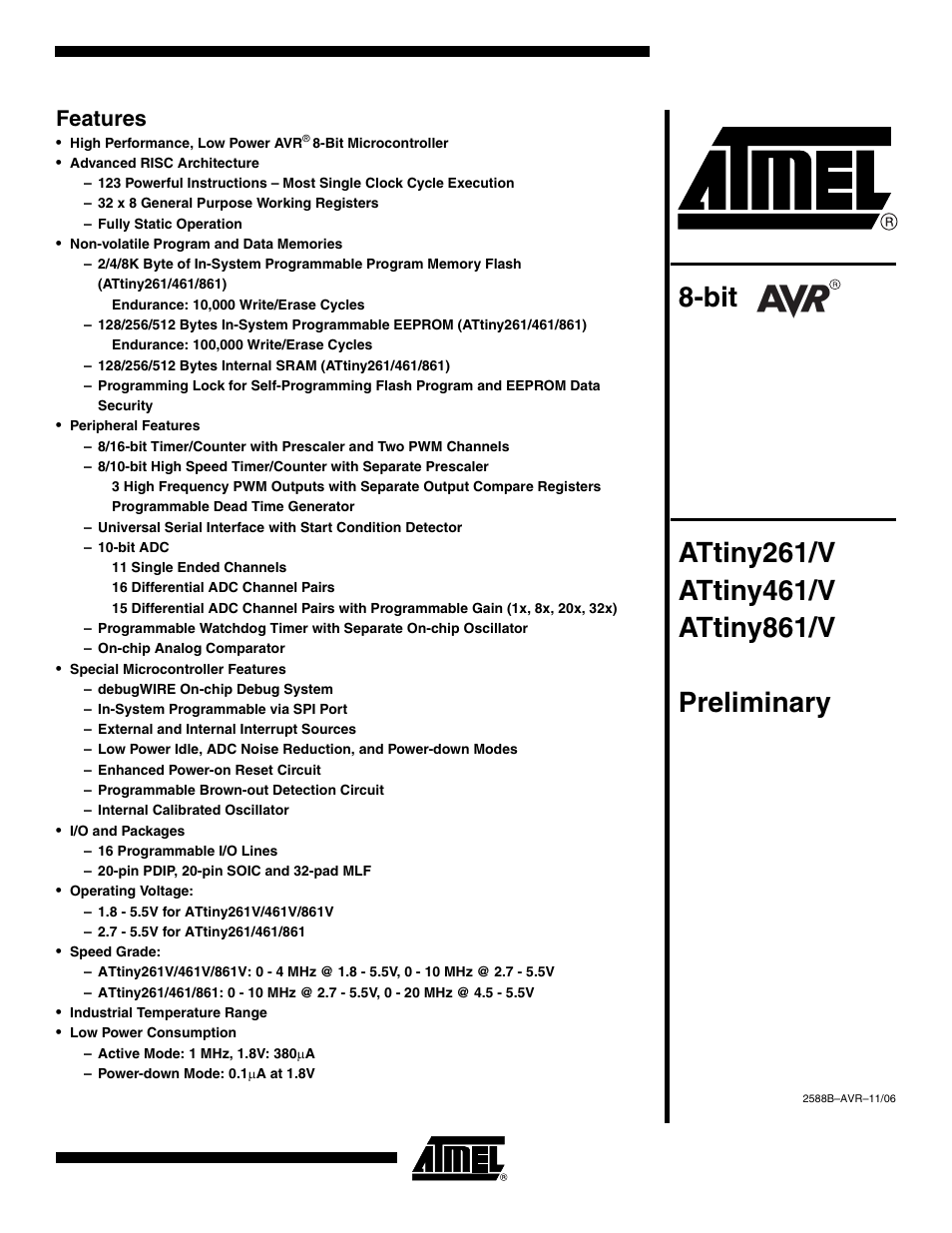
Features
Table of contents
Document Outline
- Features
- 1. Pin Configurations
- 2. Overview
- 3. Resources
- 4. About Code Examples
- 5. AVR CPU Core
- 6. AVR Memories
- 7. System Clock and Clock Options
- 7.1 Clock Systems and their Distribution
- 7.2 Clock Sources
- 7.3 Default Clock Source
- 7.4 External Clock
- 7.5 High Frequency PLL Clock - PLLCLK
- 7.6 Calibrated Internal RC Oscillator
- 7.7 128 kHz Internal Oscillator
- 7.8 Low-frequency Crystal Oscillator
- 7.9 Crystal Oscillator
- 7.10 Clock Output Buffer
- 7.11 System Clock Prescaler
- 7.12 Register Description
- 8. Power Management and Sleep Modes
- 9. System Control and Reset
- 10. Interrupts
- 11. External Interrupts
- 12. I/O Ports
- 13. Timer/Counter0 Prescaler
- 14. Timer/Counter0
- 14.1 Features
- 14.2 Overview
- 14.3 Timer/Counter Clock Sources
- 14.4 Counter Unit
- 14.5 Modes of Operation
- 14.6 Input Capture Unit
- 14.7 Output Compare Unit
- 14.8 Timer/Counter Timing Diagrams
- 14.9 Accessing Registers in 16-bit Mode
- 14.10 Register Description
- 14.10.1 TCCR0A - Timer/Counter0 Control Register A
- 14.10.2 TCNT0L - Timer/Counter0 Register Low Byte
- 14.10.3 TCNT0H - Timer/Counter0 Register High Byte
- 14.10.4 OCR0A - Timer/Counter0 Output Compare Register A
- 14.10.5 OCR0B - Timer/Counter0 Output Compare Register B
- 14.10.6 TIMSK - Timer/Counter0 Interrupt Mask Register
- 14.10.7 TIFR - Timer/Counter0 Interrupt Flag Register
- 15. Timer/Counter1 Prescaler
- 16. Timer/Counter1
- 16.1 Features
- 16.2 Overview
- 16.3 Counter Unit
- 16.4 Output Compare Unit
- 16.5 Dead Time Generator
- 16.6 Compare Match Output Unit
- 16.7 Modes of Operation
- 16.8 Timer/Counter Timing Diagrams
- 16.9 Fault Protection Unit
- 16.10 Accessing 10-Bit Registers
- 16.11 Register Description
- 16.11.1 TCCR1A - Timer/Counter1 Control Register A
- 16.11.2 TCCR1B - Timer/Counter1 Control Register B
- 16.11.3 TCCR1C - Timer/Counter1 Control Register C
- 16.11.4 TCCR1D - Timer/Counter1 Control Register D
- 16.11.5 TCCR1E - Timer/Counter1 Control Register E
- 16.11.6 TCNT1 - Timer/Counter1
- 16.11.7 TC1H - Timer/Counter1 High Byte
- 16.11.8 OCR1A - Timer/Counter1 Output Compare Register A
- 16.11.9 OCR1B - Timer/Counter1 Output Compare Register B
- 16.11.10 OCR1C - Timer/Counter1 Output Compare Register C
- 16.11.11 OCR1D - Timer/Counter1 Output Compare Register D
- 16.11.12 TIMSK - Timer/Counter1 Interrupt Mask Register
- 16.11.13 TIFR - Timer/Counter1 Interrupt Flag Register
- 16.11.14 DT1 - Timer/Counter1 Dead Time Value
- 17. USI - Universal Serial Interface
- 18. AC - Analog Comparator
- 19. ADC - Analog to Digital Converter
- 19.1 Features
- 19.2 Overview
- 19.3 Operation
- 19.4 Starting a Conversion
- 19.5 Prescaling and Conversion Timing
- 19.6 Changing Channel or Reference Selection
- 19.7 ADC Noise Canceler
- 19.8 ADC Conversion Result
- 19.9 Temperature Measurement
- 19.10 Register Descriptin
- 20. debugWIRE On-chip Debug System
- 21. Self-Programming the Flash
- 22. Memory Programming
- 22.1 Program And Data Memory Lock Bits
- 22.2 Fuse Bytes
- 22.3 Signature Bytes
- 22.4 Calibration Byte
- 22.5 Page Size
- 22.6 Parallel Programming Parameters, Pin Mapping, and Commands
- 22.7 Parallel Programming
- 22.7.1 Enter Programming Mode
- 22.7.2 Considerations for Efficient Programming
- 22.7.3 Chip Erase
- 22.7.4 Programming the Flash
- 22.7.5 Programming the EEPROM
- 22.7.6 Reading the Flash
- 22.7.7 Reading the EEPROM
- 22.7.8 Programming the Fuse Low Bits
- 22.7.9 Programming the Fuse High Bits
- 22.7.10 Programming the Extended Fuse Bits
- 22.7.11 Programming the Lock Bits
- 22.7.12 Reading the Fuse and Lock Bits
- 22.7.13 Reading the Signature Bytes
- 22.7.14 Reading the Calibration Byte
- 22.8 Serial Downloading
- 23. Electrical Characteristics
- 24. Typical Characteristics
- 24.1 Active Supply Current
- 24.2 Idle Supply Current
- 24.3 Supply Current of I/O modules
- 24.4 Power-down Supply Current
- 24.5 Pin Pull-up
- 24.6 Pin Driver Strength
- 24.7 Pin Threshold and Hysteresis
- 24.8 BOD Threshold and Analog Comparator Offset
- 24.9 Internal Oscillator Speed
- 24.10 Current Consumption of Peripheral Units
- 24.11 Current Consumption in Reset and Reset Pulsewidth
- 25. Register Summary
- 26. Instruction Set Summary
- 27. Ordering Information
- 28. Packaging Information
- 29. Errata
- 30. Datasheet Revision History
- Table of Contents

