5 didr0 - digital input disable register 0, 6 didr1 - digital input disable register 1, Didr1 – digital input dis – Rainbow Electronics ATtiny861_V User Manual
Page 160
160
2588B–AVR–11/06
ATtiny261/461/861
19.10.5
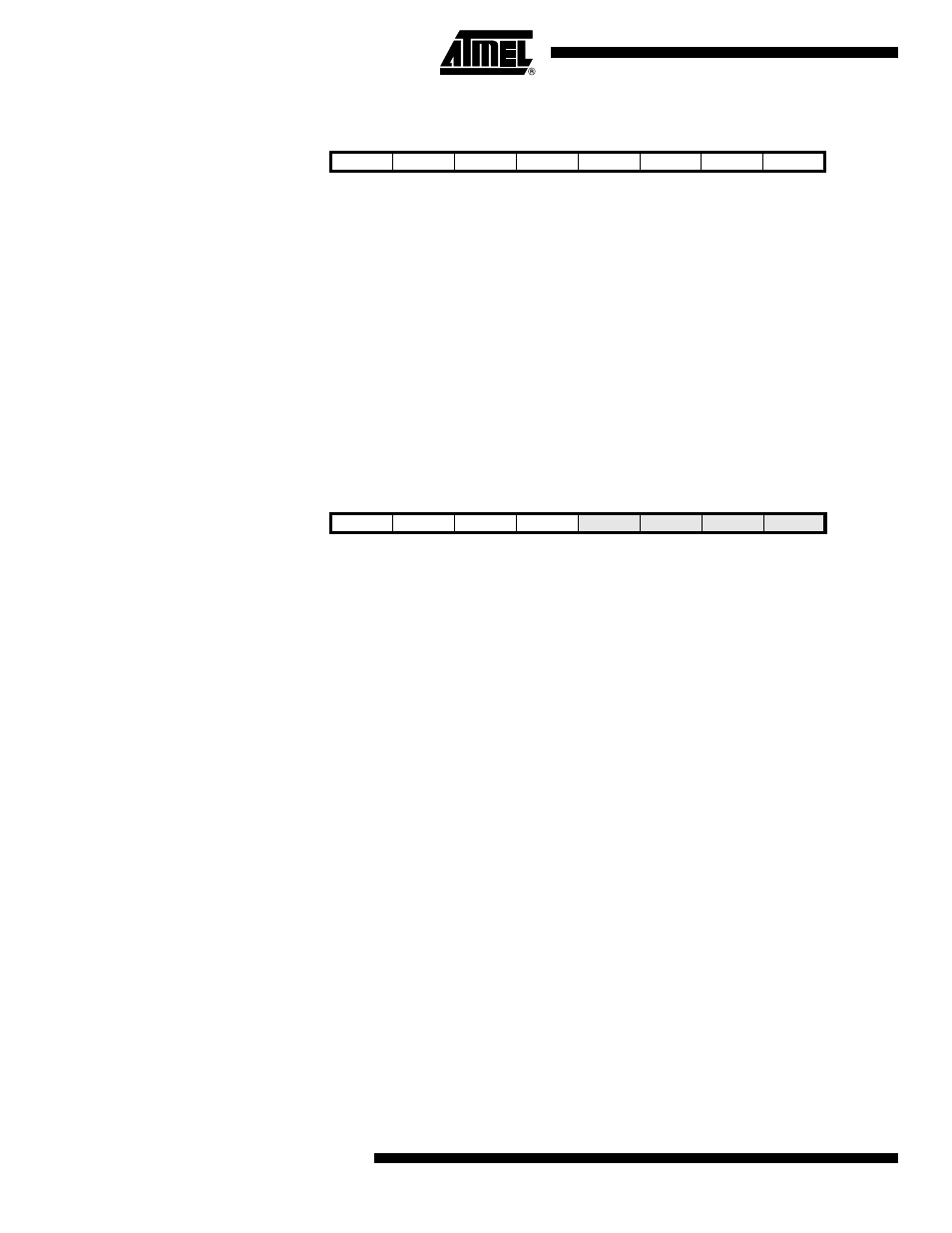
DIDR0 – Digital Input Disable Register 0
• Bits 7:4,2:0 – ADC6D:ADC0D: ADC6:0 Digital Input Disable
When this bit is written logic one, the digital input buffer on the corresponding ADC pin is dis-
abled. The corresponding PIN register bit will always read as zero when this bit is set. When an
analog signal is applied to the ADC7:0 pin and the digital input from this pin is not needed, this
bit should be written logic one to reduce power consumption in the digital input buffer.
• Bit 3 – AREFD: AREF Digital Input Disable
When this bit is written logic one, the digital input buffer on the AREF pin is disabled. The corre-
sponding PIN register bit will always read as zero when this bit is set. When an analog signal is
applied to the AREF pin and the digital input from this pin is not needed, this bit should be written
logic one to reduce power consumption in the digital input buffer.
19.10.6
DIDR1 – Digital Input Disable Register 1
• Bits 7..4 – ADC10D..ADC7D: ADC10..7 Digital Input Disable
When this bit is written logic one, the digital input buffer on the corresponding ADC pin is dis-
abled. The corresponding PIN register bit will always read as zero when this bit is set. When an
analog signal is applied to the ADC10:7 pin and the digital input from this pin is not needed, this
bit should be written logic one to reduce power consumption in the digital input buffer.
Bit
7
6
5
4
3
2
1
0
0x01 (0x21)
ADC6D
ADC5D
ADC4D
ADC3D
AREFD
ADC2D
ADC1D
ADC0D
DIDR0
Read/Write
R/W
R/W
R/W
R/W
R/W
R/W
R/W
R/W
Initial Value
0
0
0
0
0
0
0
0
Bit
7
6
5
4
3
2
1
0
0x02 (0x22)
ADC10D
ADC9D
ADC8D
ADC7D
-
DIDR1
Read/Write
R/W
R/W
R/W
R/W
R
R
R
R
Initial Value
0
0
0
0
0
0
0
0