2 analog noise canceling techniques, 3 adc accuracy definitions – Rainbow Electronics ATtiny861_V User Manual
Page 150
150
2588B–AVR–11/06
ATtiny261/461/861
19.7.2
Analog Noise Canceling Techniques
Digital circuitry inside and outside the device generates EMI which might affect the accuracy of
analog measurements. If conversion accuracy is critical, the noise level can be reduced by
applying the following techniques:
a.
Keep analog signal paths as short as possible. Make sure analog tracks run over the
analog ground plane, and keep them well away from high-speed switching digital
tracks.
b.
Use the ADC noise canceler function to reduce induced noise from the CPU.
c.
If any port pins are used as digital outputs, it is essential that these do not switch
while a conversion is in progress.
19.7.3
ADC Accuracy Definitions
An n-bit single-ended ADC converts a voltage linearly between GND and V
REF
in 2
n
steps
(LSBs). The lowest code is read as 0, and the highest code is read as 2
n
-1.
Several parameters describe the deviation from the ideal behavior:
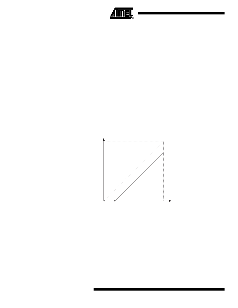
• Offset: The deviation of the first transition (0x000 to 0x001) compared to the ideal transition (at
0.5 LSB). Ideal value: 0 LSB.
Figure 19-9. Offset Error
• Gain Error: After adjusting for offset, the Gain Error is found as the deviation of the last
transition (0x3FE to 0x3FF) compared to the ideal transition (at 1.5 LSB below maximum).
Ideal value: 0 LSB
Output Code
V
REF
Input Voltage
Ideal ADC
Actual ADC
Offset
Error