Pin configurations, 1 disclaimer – Rainbow Electronics ATtiny861_V User Manual
Page 2
2
2588B–AVR–11/06
ATtiny261/461/861
1.
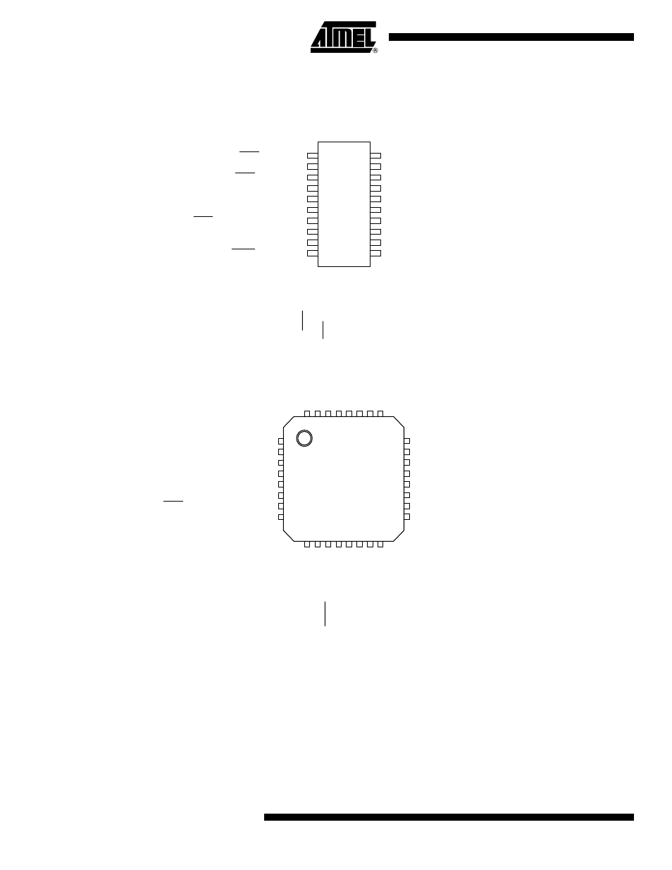
Pin Configurations
Figure 1-1.
Pinout ATtiny261/461/861
Note:
The large center pad underneath the QFN/MLF package should be soldered to ground on the board to ensure good mechanical
stability.
1.1
Disclaimer
Typical values contained in this data sheet are based on simulations and characterization of other AVR microcontrollers
manufactured on the same process technology. Min and Max values will be available after the device is characterized.
1
2
3
4
5
6
7
8
9
10
20
19
18
17
16
15
14
13
12
11
(MOSI/DI/SDA/OC1A/PCINT8) PB0
(MISO/DO/OC1A/PCINT9) PB1
(SCK/USCK/SCL/OC1B/PCINT10) PB2
(OC1B/PCINT11) PB3
VCC
GND
(ADC7/OC1D/CLKI/XTAL1/PCINT12) PB4
(ADC8/OC1D/CLKO/XTAL2/PCINT13) PB5
(ADC9/INT0/T0/PCINT14) PB6
(ADC10/RESET/PCINT15) PB7
PA0 (ADC0/DI/SDA/PCINT0)
PA1 (ADC1/DO/PCINT1)
PA2 (ADC2/INT1/USCK/SCL/PCINT2)
PA3 (AREF/PCINT3)
AGND
AVCC
PA4 (ADC3/ICP0/PCINT4)
PA5 (ADC4/AIN2/PCINT5)
PA6 (ADC5/AIN0/PCINT6)
PA7 (ADC6/AIN1/PCINT7)
PDIP/SOIC
1
2
3
4
5
6
7
8
24
23
22
21
20
19
18
17
32
31
30
29
28
27
26
25
9
10
11
12
13
14
15
16
NC
(OC1B/PCINT11) PB3
NC
VCC
GND
NC
(ADC7/OC1D/CLKI/XTAL1/PCINT12) PB4
(ADC8/OC1D/CLKO/XTAL2/PCINT13) PB5
NC
PA2 (ADC2/INT1/USCK/SCL/PCINT2)
PA3 (AREF/PCINT3)
AGND
NC
NC
AVCC
PA4 (ADC3/ICP0/PCINT4)
NC
(ADC9/INT0/T0/PCINT14) PB6
(ADC10/RESET/PCINT15) PB7
NC
(ADC6/AIN1/PCINT7) PA7
(ADC5/AIN0/PCINT6) PA6
(ADC4/AIN2/PCINT5) PA5
NC
PB2 (SCK/USCK/SCL/OC1B/PCINT10)
PB1 (MISO/DO/OC1A/PCINT9)
PB0 (MOSI/DI/SDA/OC1A/PCINT8)
NC
NC
NC
PA0 (ADC0/DI/SDA/PCINT0)
PA1 (ADC1/DO/PCINT1)
QFN/MLF