10 register descriptin, 1 admux - adc multiplexer selection register – Rainbow Electronics ATtiny861_V User Manual
Page 154
154
2588B–AVR–11/06
ATtiny261/461/861
where ADCn are the ADC data registers, k is a fixed coefficient and T
OS
is the temperature sen-
sor offset value determined and stored into EEPROM.
19.10 Register Descriptin
19.10.1
ADMUX – ADC Multiplexer Selection Register
• Bit 7:6 – REFS1:REFS0: Voltage Reference Selection Bits
These bits and the REFS2 bit from the ADC Control and Status Register B (ADCSRB) select the
voltage reference for the ADC, as shown in
Table 19-3
. If these bits are changed during a
conversion, the change will not go in effect until this conversion is complete (ADIF in ADCSR is
set). Whenever these bits are changed, the next conversion will take 25 ADC clock cycles. If
active channels are used, using AVCC or an external AREF higher than (AVCC - 1V) is not
recommended, as this will affect ADC accuracy. The internal voltage reference options may not
be used if an external voltage is being applied to the AREF pin.
•
Bit 5 – ADLAR: ADC Left Adjust Result
The ADLAR bit affects the presentation of the ADC conversion result in the ADC Data Register.
Write one to ADLAR to left adjust the result. Otherwise, the result is right adjusted. Changing the
ADLAR bit will affect the ADC Data Register immediately, regardless of any ongoing conver-
sions. For a comple te description of this bit, see
”ADCL and ADCH – The ADC Data Register”
.
• Bits 4:0 – MUX4:0: Analog Channel and Gain Selection Bits
These bits and the MUX5 bit from the ADC Control and Status Register B (ADCSRB) select
which combination of analog inputs are connected to the ADC. In case of differential input, gain
selection is also made with these bits. Selecting the same pin as both inputs to the differential
gain stage enables offset measurements. Selecting the single-ended channel ADC11 enables
the temperature sensor. Refer to
Table 19-4
for details. If these bits are changed during a
conversion, the change will not go into effect until this conversion is complete (ADIF in ADCSRA
is set).
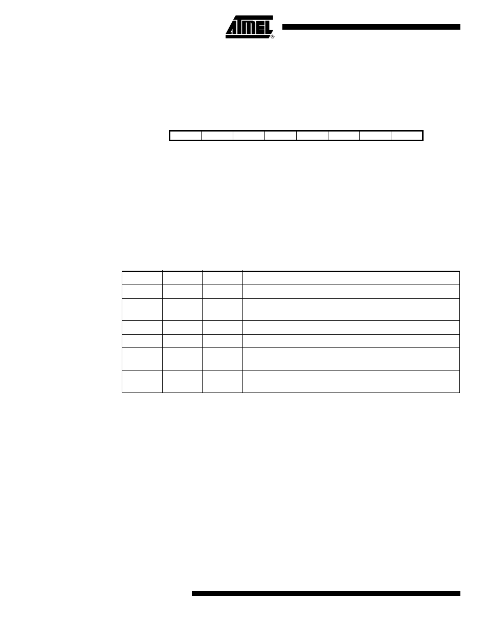
Bit
7
6
5
4
3
2
1
0
0x07 (0x27)
REFS1
REFS0
ADLAR
MUX4
MUX3
MUX2
MUX1
MUX0
ADMUX
Read/Write
R/W
R/W
R/W
R/W
R/W
R/W
R/W
R/W
Initial Value
0
0
0
0
0
0
0
0
Table 19-3.
Voltage Reference Selections for ADC
REFS2
REFS1
REFS0
Voltage Reference (V
REF
) Selection
X
0
0
V
CC
used as Voltage Reference, disconnected from AREF.
X
0
1
External Voltage Reference at AREF pin, Internal Voltage
Reference turned off.
0
1
0
Internal 1.1V Voltage Reference.
0
1
1
Reserved.
1
1
0
Internal 2.56V Voltage Reference without external bypass
capacitor, disconnected from AREF.
1
1
1
Internal 2.56V Voltage Reference with external bypass capacitor
at AREF pin.