5 usipp - usi pin position – Rainbow Electronics ATtiny861_V User Manual
Page 137
137
2588B–AVR–11/06
ATtiny261/461/861
• Bit 1 – USICLK: Clock Strobe
Writing a one to this bit location strobes the USI Data Register to shift one step and the counter
to increment by one, provided that the USICS1..0 bits are set to zero and by doing so the soft-
ware clock strobe option is selected. The output will change immediately when the clock strobe
is executed, i.e., in the same instruction cycle. The value shifted into the USI Data Register is
sampled the previous instruction cycle. The bit will be read as zero.
When an external clock source is selected (USICS1 = 1), the USICLK function is changed from
a clock strobe to a Clock Select Register. Setting the USICLK bit in this case will select the
USITC strobe bit as clock source for the 4-bit counter (see
Table 17-2
).
• Bit 0 – USITC: Toggle Clock Port Pin
Writing a one to this bit location toggles the USCK/SCL value either from 0 to 1, or from 1 to 0.
The toggling is independent of the setting in the Data Direction Register, but if the PORT value is
to be shown on the pin the DDB2 must be set as output (to one). This feature allows easy clock
generation when implementing master devices. The bit will be read as zero.
When an external clock source is selected (USICS1 = 1) and the USICLK bit is set to one, writ-
ing to the USITC strobe bit will directly clock the 4-bit counter. This allows an early detection of
when the transfer is done when operating as a master device.
17.5.5
USIPP – USI Pin Position
• Bits 7:1 – Res: Reserved Bits
These bits are reserved bits in the ATtiny261/461/861 and always reads as zero.
• Bit 0 – USIPOS: USI Pin Position
Setting this bit to one changes the USI pin position. As default pins PB2..PB0 are used for the
USI pin functions, but when writing this bit to one the USIPOS bit is set the USI pin functions are
on pins PA2..PA0.
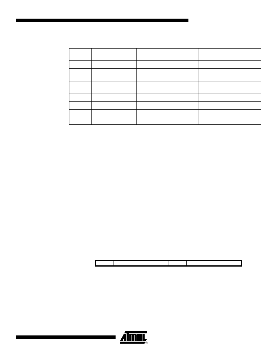
Table 17-2.
Relations between the USICS1..0 and USICLK Setting
USICS1
USICS0
USICLK
USI Data Register Clock
Source
4-bit Counter Clock Source
0
0
0
No Clock
No Clock
0
0
1
Software clock strobe
(USICLK)
Software clock strobe
(USICLK)
0
1
X
Timer/Counter0 Compare
Match
Timer/Counter0 Compare
Match
1
0
0
External, positive edge
External, both edges
1
1
0
External, negative edge
External, both edges
1
0
1
External, positive edge
Software clock strobe (USITC)
1
1
1
External, negative edge
Software clock strobe (USITC)
Bit
7
6
5
4
3
2
1
0
0x11 (0x31)
-
-
-
-
-
-
-
USIPOS
USIPP
Read/Write
R
R
R
R
R
R
R
R/W
Initial Value
0
0
0
0
0
0
0
0