Memory programming, 1 program and data memory lock bits, Contains – Rainbow Electronics ATtiny861_V User Manual
Page 168
168
2588B–AVR–11/06
ATtiny261/461/861
22. Memory Programming
This section describes the different methods for Programming the ATtiny261/461/861 memories.
22.1
Program And Data Memory Lock Bits
The ATtiny261/461/861 provides two Lock bits which can be left unprogrammed (“1”) or can be
programmed (“0”) to obtain the additional security listed in
Table 22-2
. The Lock bits can only be
erased to “1” with the Chip Erase command. The ATtiny261/461/861 has no separate Boot
Loader section. The SPM instruction is enabled for the whole Flash, if the SELFPROGEN fuse is
programmed (“0”), otherwise it is disabled.
Note:
1. “1” means unprogrammed, “0” means programmed
Notes:
1. Program the Fuse bits before programming the LB1 and LB2.
2. “1” means unprogrammed, “0” means programmed
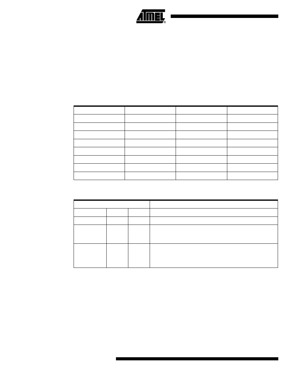
Table 22-1.
Lock Bit Byte
(1)
Lock Bit Byte
Bit No
Description
Default Value
7
–
1 (unprogrammed)
6
–
1 (unprogrammed)
5
–
1 (unprogrammed)
4
–
1 (unprogrammed)
3
–
1 (unprogrammed)
2
–
1 (unprogrammed)
LB2
1
Lock bit
1 (unprogrammed)
LB1
0
Lock bit
1 (unprogrammed)
Table 22-2.
Lock Bit Protection Modes
(1)(2)
Memory Lock Bits
Protection Type
LB Mode
LB2
LB1
1
1
1
No memory lock features enabled.
2
1
0
Further programming of the Flash and EEPROM is disabled in
High-voltage and Serial Programming mode. The Fuse bits are
locked in both Serial and High-voltage Programming mode.
(1)
3
0
0
Further programming and verification of the Flash and EEPROM
is disabled in High-voltage and Serial Programming mode. The
Fuse bits are locked in both Serial and High-voltage
Programming mode.
(1)