4 usicr - usi control register – Rainbow Electronics ATtiny861_V User Manual
Page 135
135
2588B–AVR–11/06
ATtiny261/461/861
The 4-bit counter increments by one for each clock generated either by the external clock edge
detector, by a Timer/Counter0 Compare Match, or by software using USICLK or USITC strobe
bits. The clock source depends of the setting of the USICS1..0 bits. For external clock operation
a special feature is added that allows the clock to be generated by writing to the USITC strobe
bit. This feature is enabled by write a one to the USICLK bit while setting an external clock
source (USICS1 = 1).
Note that even when no wire mode is selected (USIWM1..0 = 0) the external clock input
(USCK/SCL) are can still be used by the counter.
17.5.4
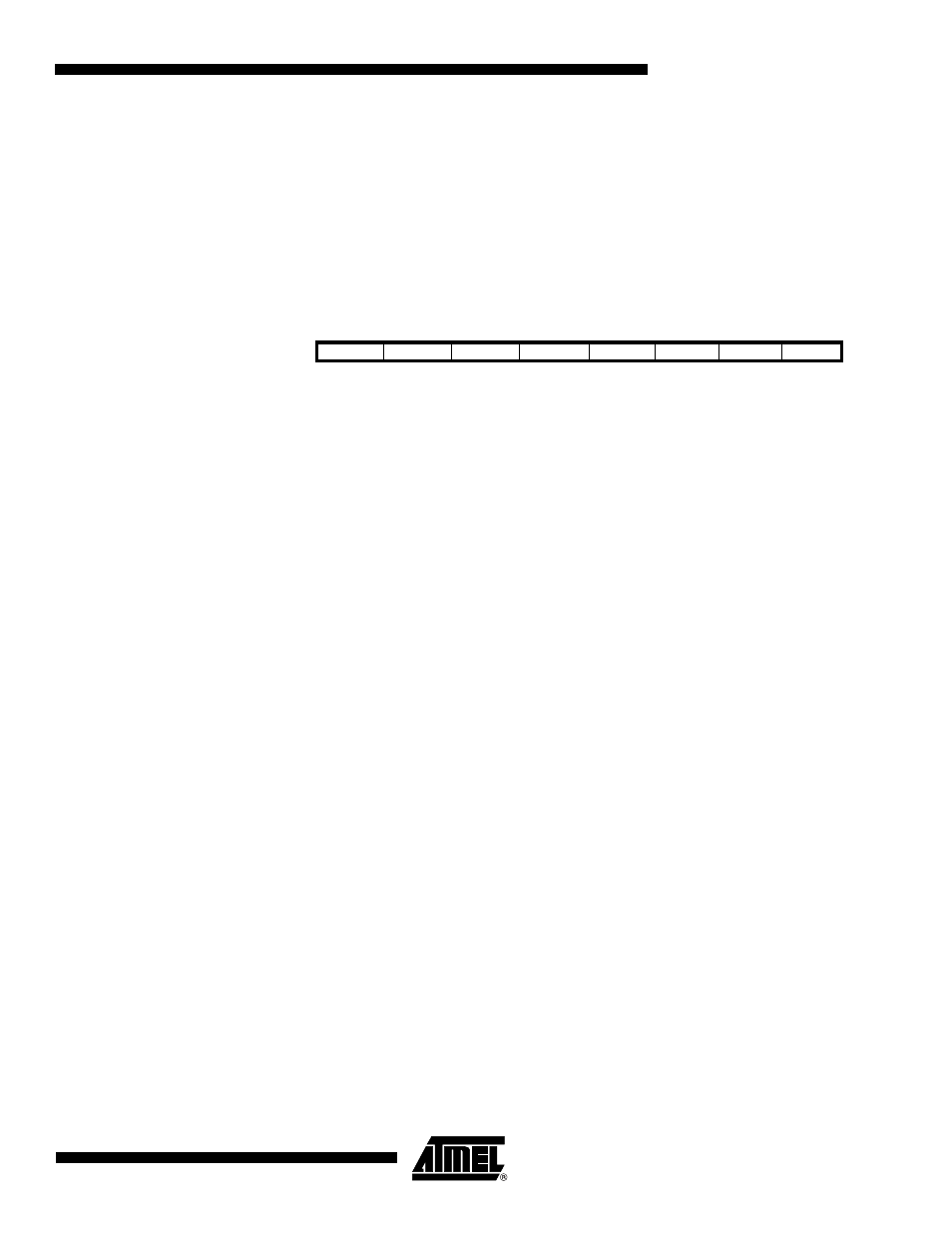
USICR – USI Control Register
The Control Register includes interrupt enable control, wire mode setting, Clock Select setting,
and clock strobe.
• Bit 7 – USISIE: Start Condition Interrupt Enable
Setting this bit to one enables the Start Condition detector interrupt. If there is a pending inter-
rupt when the USISIE and the Global Interrupt Enable Flag is set to one, this will immediately be
executed. Refer to the USISIF bit description on page 134 for further details.
• Bit 6 – USIOIE: Counter Overflow Interrupt Enable
Setting this bit to one enables the Counter Overflow interrupt. If there is a pending interrupt when
the USIOIE and the Global Interrupt Enable Flag is set to one, this will immediately be executed.
Refer to the USIOIF bit description on page 134 for further details.
• Bit 5:4 – USIWM1:0: Wire Mode
These bits set the type of wire mode to be used. Basically only the function of the outputs are
affected by these bits. Data and clock inputs are not affected by the mode selected and will
always have the same function. The counter and USI Data Register can therefore be clocked
externally, and data input sampled, even when outputs are disabled. The relations between
USIWM1:0 and the USI operation is summarized in
Table 17-1
.
Bit
7
6
5
4
3
2
1
0
0x0D (0x2D)
USISIE
USIOIE
USIWM1
USIWM0
USICS1
USICS0
USICLK
USITC
USICR
Read/Write
R/W
R/W
R/W
R/W
R/W
R/W
W
W
Initial Value
0
0
0
0
0
0
0
0