8 timer/counter timing diagrams – Rainbow Electronics ATtiny861_V User Manual
Page 107
107
2588B–AVR–11/06
ATtiny261/461/861
and, if the Override Enable bit is set, the Output Compare pin is allowed to be connected on the
port pin. The Output Compare Pin configurations are described in
Table 16-5
.
16.8
Timer/Counter Timing Diagrams
The Timer/Counter is a synchronous design and the timer clock (clk
T1
) is therefore shown as a
clock enable signal in the following figures. The figures include information on when Interrupt
Flags are set.
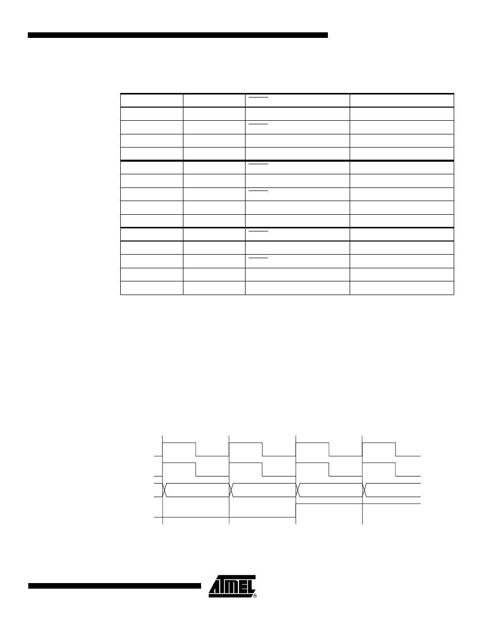
Figure 16-14
contains timing data for basic Timer/Counter operation. The figure shows the count
sequence close to the MAX value in all modes other than Phase and Frequency Correct PWM
Mode.
Figure 16-15
shows the same timing data, but with the prescaler enabled, in all modes
other than Phase and Frequency Correct PWM Mode.
Figure 16-16
shows the setting of
OCF1A, OCF1B and OCF1D in all modes, and
Figure 16-17
shows the setting of TOV1 in
Phase and Frequency Correct PWM Mode.
Figure 16-14. Timer/Counter Timing Diagram, no Prescaling
Table 16-5.
Output Compare Pin configurations in PWM6 Mode
COM1A1
COM1A0
OC1A Pin (PB0)
OC1A Pin (PB1)
0
0
Disconnected
Disconnected
0
1
OC1A •
OC1OE0
OC1A •
OC1OE1
1
0
OC1A •
OC1OE0
OC1A •
OC1OE1
1
1
OC1A •
OC1OE0
OC1A •
OC1OE1
COM1B1
COM1B0
OC1B Pin (PB2)
OC1B Pin (PB3)
0
0
Disconnected
Disconnected
0
1
OC1A •
OC1OE2
OC1A •
OC1OE3
1
0
OC1A •
OC1OE2
OC1A •
OC1OE3
1
1
OC1A •
OC1OE2
OC1A •
OC1OE3
COM1D1
COM1D0
OC1D Pin (PB4)
OC1D Pin (PB5)
0
0
Disconnected
Disconnected
0
1
OC1A •
OC1OE4
OC1A •
OC1OE5
1
0
OC1A •
OC1OE4
OC1A •
OC1OE5
1
1
OC1A •
OC1OE4
OC1A •
OC1OE5
clk
Tn
(clk
PCK
/1)
TOVn
clk
PCK
TCNTn
TOP - 1
TOP
BOTTOM
BOTTOM + 1