Timer/counter0 prescaler, 1 prescaler reset, 2 external clock source – Rainbow Electronics ATtiny861_V User Manual
Page 69
69
2588B–AVR–11/06
ATtiny261/461/861
13. Timer/Counter0 Prescaler
The Timer/Counter can be clocked directly by the system clock (by setting the CSn2:0 = 1). This
provides the fastest operation, with a maximum Timer/Counter clock frequency equal to system
clock frequency (f
CLK_I/O
). Alternatively, one of four taps from the prescaler can be used as a
clock source. The prescaled clock has a frequency of either f
CLK_I/O
/8, f
CLK_I/O
/64, f
CLK_I/O
/256, or
f
CLK_I/O
/1024. See
for details.
13.0.1
Prescaler Reset
The prescaler is free running, i.e., operates independently of the Clock Select logic of the
Timer/Counter. Since the prescaler is not affected by the Timer/Counter’s clock select, the state
of the prescaler will have implications for situations where a prescaled clock is used. One exam-
ple of prescaling artifacts occurs when the timer is enabled and clocked by the prescaler (6 >
CSn2:0 > 1). The number of system clock cycles from when the timer is enabled to the first count
occurs can be from 1 to N+1 system clock cycles, where N equals the prescaler divisor (8, 64,
256, or 1024). It is possible to use the Prescaler Reset for synchronizing the Timer/Counter to
program execution.
13.0.2
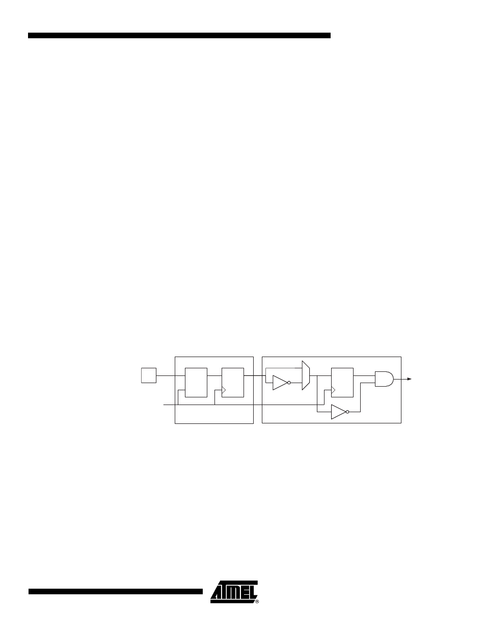
External Clock Source
An external clock source applied to the T0 pin can be used as Timer/Counter clock (clk
T0
). The
T0 pin is sampled once every system clock cycle by the pin synchronization logic. The synchro-
nized (sampled) signal is then passed through the edge detector.
shows a functional
equivalent block diagram of the T0 synchronization and edge detector logic. The registers are
clocked at the positive edge of the internal system clock (
clk
I/O
). The latch is transparent in the
high period of the internal system clock.
The edge detector generates one clk
T
0
pulse for each positive (CSn2:0 = 7) or negative (CSn2:0
for details.
Figure 13-1. T0 Pin Sampling
The synchronization and edge detector logic introduces a delay of 2.5 to 3.5 system clock cycles
from an edge has been applied to the T0 pin to the counter is updated.
Enabling and disabling of the clock input must be done when T0 has been stable for at least one
system clock cycle, otherwise it is a risk that a false Timer/Counter clock pulse is generated.
Each half period of the external clock applied must be longer than one system clock cycle to
ensure correct sampling. The external clock must be guaranteed to have less than half the sys-
tem clock frequency (f
ExtClk
< f
clk_I/O
/2) given a 50/50% duty cycle. Since the edge detector uses
sampling, the maximum frequency of an external clock it can detect is half the sampling fre-
quency (Nyquist sampling theorem). However, due to variation of the system clock frequency
and duty cycle caused by Oscillator source (crystal, resonator, and capacitors) tolerances, it is
recommended that maximum frequency of an external clock source is less than f
clk_I/O
/2.5.
Tn_sync
(To Clock
Select Logic)
Edge Detector
Synchronization
D
Q
D
Q
LE
D
Q
Tn
clk
I/O