Ac - analog comparator, 1 register description, Ac – analog comparator – Rainbow Electronics ATtiny861_V User Manual
Page 138
138
2588B–AVR–11/06
ATtiny261/461/861
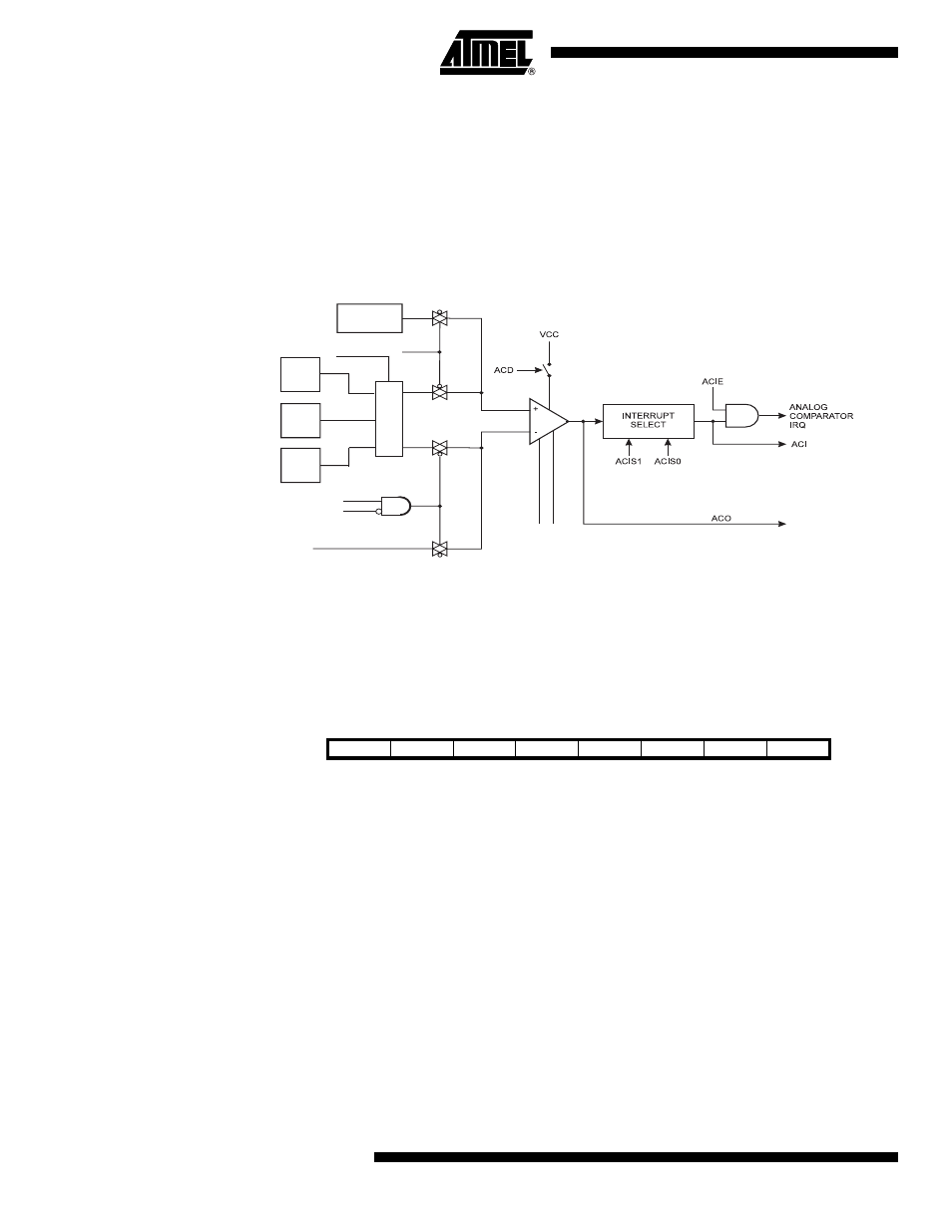
18. AC – Analog Comparator
The Analog Comparator compares the input values on the selectable positive pin (AIN0, AIN1 or
AIN2) and selectable negative pin (AIN0, AIN1 or AIN2). When the voltage on the positive pin is
higher than the voltage on the negative pin, the Analog Comparator output, ACO, is set. The
comparator can trigger a separate interrupt, exclusive to the Analog Comparator. The user can
select Interrupt triggering on comparator output rise, fall or toggle. A block diagram of the com-
parator and its surrounding logic is shown in
Figure 18-1
.
Figure 18-1. Analog Comparator Block Diagram
(2)
Notes:
1. See
2. Refer to
Figure 1-1 on page 2
and
for Analog Comparator pin
placement.
18.1
Register Description
18.1.1
ACSRA – Analog Comparator Control and Status Register A
• Bit 7 – ACD: Analog Comparator Disable
When this bit is written logic one, the power to the Analog Comparator is switched off. This bit
can be set at any time to turn off the Analog Comparator. This will reduce power consumption in
Active and Idle mode. When changing the ACD bit, the Analog Comparator Interrupt must be
disabled by clearing the ACIE bit in ACSRA. Otherwise an interrupt can occur when the bit is
changed.
• Bit 6 – ACBG: Analog Comparator Bandgap Select
When this bit is set an internal 1.1V reference voltage replaces the positive input to the Analog
Comparator. The selection of the internal voltage reference is done by writing the REFS2..0 bits
in ADMUX register. When this bit is cleared, AIN0, AIN1 or AIN2 depending on the ACM2..0 bits
is applied to the positive input of the analog comparator.
ACBG
BANDGAP
REFERENCE
ADC MULTIPLEXER
OUTPUT
ACME
ADEN
(1)
MUX
AIN0
AIN1
AIN2
ACM2..1
HSEL
HLEV
Bit
7
6
5
4
3
2
1
0
0x08 (0x28)
ACD
ACBG
ACO
ACI
ACIE
ACME
ACIS1
ACIS0
ACSRA
Read/Write
R/W
R/W
R
R/W
R/W
R/W
R/W
R/W
Initial Value
0
0
N/A
0
0
0
0
0