6 timsk - timer/counter0 interrupt mask register – Rainbow Electronics ATtiny861_V User Manual
Page 86
86
2588B–AVR–11/06
ATtiny261/461/861
In 16-bit mode the OCR0B register contains the high byte of the 16-bit Output Compare Regis-
ter. To ensure that both the high and the low bytes are written simultaneously when the CPU
writes to these registers, the access is performed using an 8-bit temporary high byte register
(TEMP). This temporary register is shared by all the other 16-bit registers. See
isters in 16-bit Mode” on page 80
.
14.10.6
TIMSK – Timer/Counter0 Interrupt Mask Register
• Bit 4 – OCIE0A: Timer/Counter0 Output Compare Match A Interrupt Enable
When the OCIE0A bit is written to one, and the I-bit in the Status Register is set, the
Timer/Counter0 Compare Match A interrupt is enabled. The corresponding interrupt is executed
if a Compare Match in Timer/Counter0 occurs, i.e., when the OCF0A bit is set in the
Timer/Counter 0 Interrupt Flag Register – TIFR0.
• Bit 3 – OCIE0B: Timer/Counter Output Compare Match B Interrupt Enable
When the OCIE0B bit is written to one, and the I-bit in the Status Register is set, the
Timer/Counter Compare Match B interrupt is enabled. The corresponding interrupt is executed if
a Compare Match in Timer/Counter occurs, i.e., when the OCF0B bit is set in the Timer/Counter
Interrupt Flag Register – TIFR0.
• Bit 1 – TOIE0: Timer/Counter0 Overflow Interrupt Enable
When the TOIE0 bit is written to one, and the I-bit in the Status Register is set, the
Timer/Counter0 Overflow interrupt is enabled. The corresponding interrupt is executed if an
overflow in Timer/Counter0 occurs, i.e., when the TOV0 bit is set in the Timer/Counter 0 Inter-
rupt Flag Register – TIFR0.
• Bit 0 – TICIE0: Timer/Counter0, Input Capture Interrupt Enable
When this bit is written to one, and the I-flag in the Status Register is set (interrupts globally
enabled), the Timer/Counter1 Input Capture interrupt is enabled. The corresponding Interrupt
Vector (
) is executed when the ICF0 flag, located in TIFR, is set.
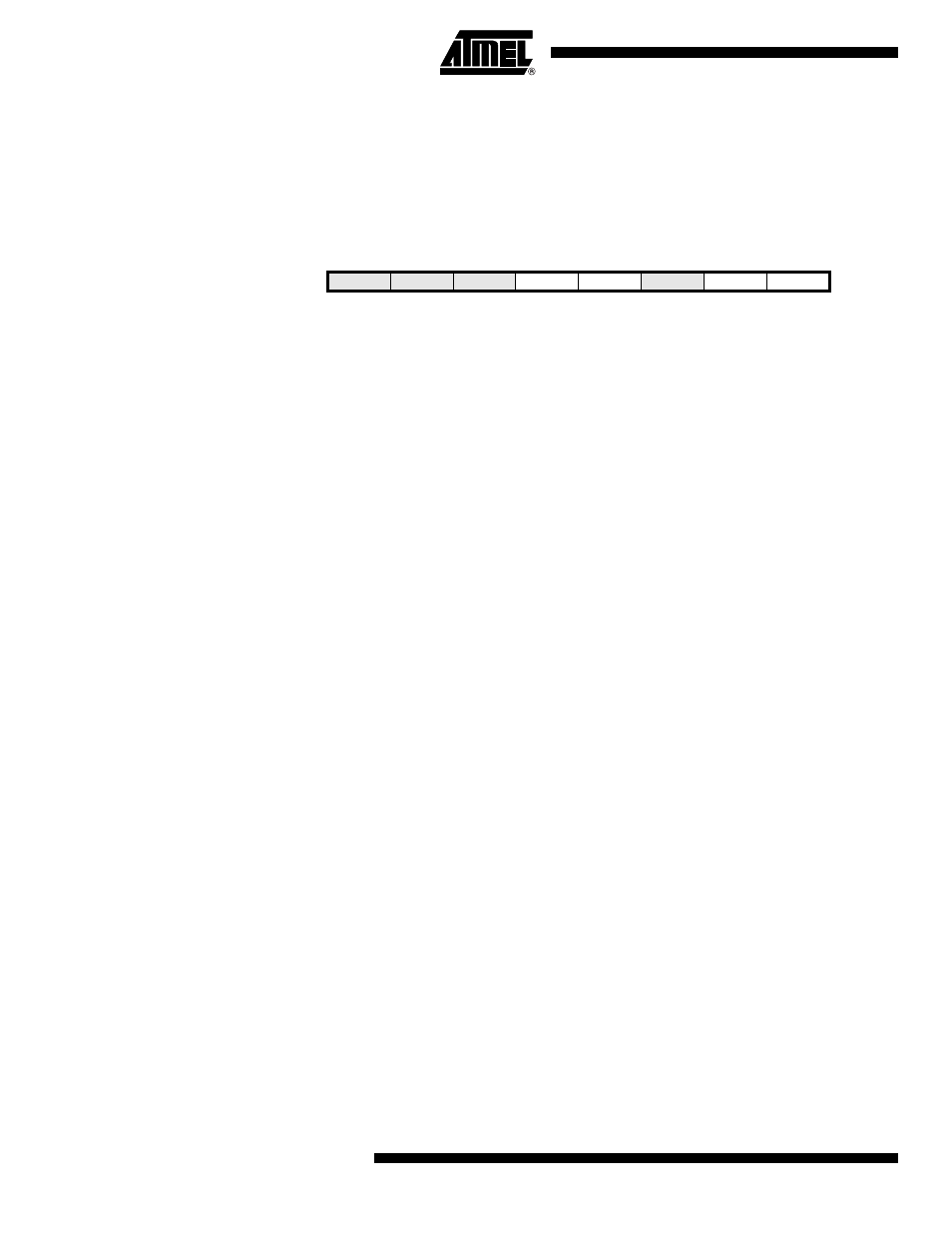
Bit
7
6
5
4
3
2
1
0
0x39 (0x59)
OCIE1D
OCIE1A
OCIE1B
OCIE0A
OCIE0B
TOIE1
TOIE0
TICIE0
TIMSK
Read/Write
R/W
R/W
R/W
R/W
R/W
R/W
R/W
R
Initial Value
0
0
0
0
0
0
0
0