Rainbow Electronics ATtiny861_V User Manual
Page 106
106
2588B–AVR–11/06
ATtiny261/461/861
Output at the timer clock cycle the counter is cleared (changes from TOP to BOTTOM). The
Timer/Counter Overflow Flag (TOV1) is set each time the counter reaches the TOP and, if the
interrupt is enabled, the interrupt handler routine can be used for updating the compare value.
Whereas, if the dual-slope operation is selected (the WGM10 bit is set to 1), the counter counts
repeatedly from BOTTOM to TOP (defined as OCR1C) and then from TOP to BOTTOM like in
Phase and Frequency Correct PWM Mode. The PWM waveform is generated by setting (or
clearing) the Waveforn Output (OCW1A) at the Compare Match between OCR1A and TCNT1
when the counter increments, and clearing (or setting) the Waveform Output at the he Compare
Match between OCR1A and TCNT1 when the counter decrements. The Timer/Counter Overflow
Flag (TOV1) is set each time the counter reaches the BOTTOM and, if the interrupt is enabled,
the interrupt handler routine can be used for updating the compare value.
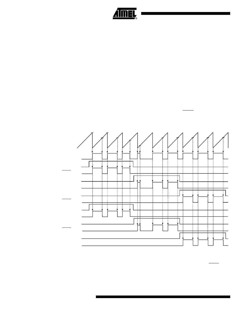
The timing diagram for the PWM6 Mode in single-slope operation (WGM11 = 0) when the
COM1A1:0 bits are set to “10” is shown in
. The counter is incremented until the
counter value matches the TOP value. The counter is then cleared at the following timer clock
cycle. The TCNT1 value is in the timing diagram shown as a histogram for illustrating the single-
slope operation. The timing diagram includes Output Compare pins OC1A and OC1A, and the
corresponding Output Compare Override Enable bits (OC1OE1..OC1OE0).
Figure 16-13. PWM6 Mode, Single-slope Operation, Timing Diagram
The general I/O port function is overridden by the Output Compare value (OC1x / OC1x) from
the Dead Time Generator if either of the COM1x1:0 bits are set. The Output Compare pins can
also be overriden by the Output Compare Override Enable bits OC1OE5..OC1OE0. If an Over-
ride Enable bit is cleared, the actual value from the port register will be visible on the port pin
TCNT1
OC1A Pin
OC1A Pin
OC1B Pin
OC1B Pin
OC1D Pin
OC1D Pin
OC1OE0
OC1OE1
OC1OE2
OC1OE3
OC1OE4
OC1OE5
OCW1A