2 serial programming instruction set – Rainbow Electronics ATtiny861_V User Manual
Page 183
183
2588B–AVR–11/06
ATtiny261/461/861
22.8.2
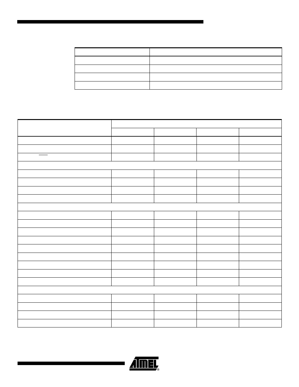
Serial Programming Instruction set
Table 22-15 on page 183
and
Figure 22-8 on page 184
describes the Instruction set.
Table 22-14. Minimum Wait Delay Before Writing the Next Flash or EEPROM Location
Symbol
Minimum Wait Delay
t
WD_FLASH
4.5 ms
t
WD_EEPROM
4.0 ms
t
WD_ERASE
4.0 ms
t
WD_FUSE
4.5 ms
Table 22-15. Serial Programming Instruction Set
Instruction/Operation
Instruction Format
Byte 1
Byte 2
Byte 3
Byte4
Programming Enable
$AC
$53
$00
$00
Chip Erase (Program Memory/EEPROM)
$AC
$80
$00
$00
Poll RDY/BSY
$F0
$00
$00
data byte out
Load Instructions
Load Extended Address byte
$4D
$00
Extended adr
$00
Load Program Memory Page, High byte
$48
adr MSB
adr LSB
high data byte in
Load Program Memory Page, Low byte
$40
adr MSB
adr LSB
low data byte in
Load EEPROM Memory Page (page access)
$C1
$00
0000 000aa
data byte in
Read Instructions
Read Program Memory, High byte
$28
adr MSB
adr LSB
high data byte out
Read Program Memory, Low byte
$20
adr MSB
adr LSB
low data byte out
Read EEPROM Memory
$A0
$00
00aa aaaa
data byte out
Read Lock bits
$58
$00
$00
data byte out
Read Signature Byte
$30
$00
0000 000aa
data byte out
Read Fuse bits
$50
$00
$00
data byte out
Read Fuse High bits
$58
$08
$00
data byte out
Read Extended Fuse Bits
$50
$08
$00
data byte out
Read Calibration Byte
$38
$00
$00
data byte out
Write Instructions
Write Program Memory Page
$4C
adr MSB
adr LSB
$00
Write EEPROM Memory
$C0
$00
00aa aaaa
data byte in
Write EEPROM Memory Page (page access)
$C2
$00
00aa aa00
$00
Write Lock bits
$AC
$E0
$00
data byte in