4 tccr1d - timer/counter1 control register d – Rainbow Electronics ATtiny861_V User Manual
Page 119

119
2588B–AVR–11/06
ATtiny261/461/861
• Bit 1 - FOC1D: Force Output Compare Match 1D
The FOC1D bit is only active when the PWM1D bit specify a non-PWM mode.
Writing a logical one to this bit forces a change in the Waveform Output (OCW1D) and the Out-
put Compare pin (OC1D) according to the values already set in COM1D1 and COM1D0. If
COM1D1 and COM1D0 written in the same cycle as FOC1D, the new settings will be used. The
Force Output Compare bit can be used to change the output pin value regardless of the timer
value. The automatic action programmed in COM1D1 and COM1D0 takes place as if a compare
match had occurred, but no interrupt is generated. The FOC1D bit is always read as zero.
• Bit 0 - PWM1D: Pulse Width Modulator D Enable
When set (one) this bit enables PWM mode based on comparator OCR1D.
16.11.4
TCCR1D – Timer/Counter1 Control Register D
• Bit 7 - FPIE1: Fault Protection Interrupt Enable
Setting this bit (to one) enables the Fault Protection Interrupt.
• Bit 6– FPEN1: Fault Protection Mode Enable
Setting this bit (to one) activates the Fault Protection Mode.
• Bit 5 – FPNC1: Fault Protection Noise Canceler
Setting this bit activates the Fault Protection Noise Canceler. When the noise canceler is acti-
vated, the input from the Fault Protection Pin (INT0) is filtered. The filter function requires four
successive equal valued samples of the INT0 pin for changing its output. The Fault Protection is
therefore delayed by four Oscillator cycles when the noise canceler is enabled.
• Bit 4 – FPES1: Fault Protection Edge Select
This bit selects which edge on the Fault Protection pin (INT0) is used to trigger a fault event.
When the FPES1 bit is written to zero, a falling (negative) edge is used as trigger, and when the
FPES1 bit is written to one, a rising (positive) edge will trigger the fault.
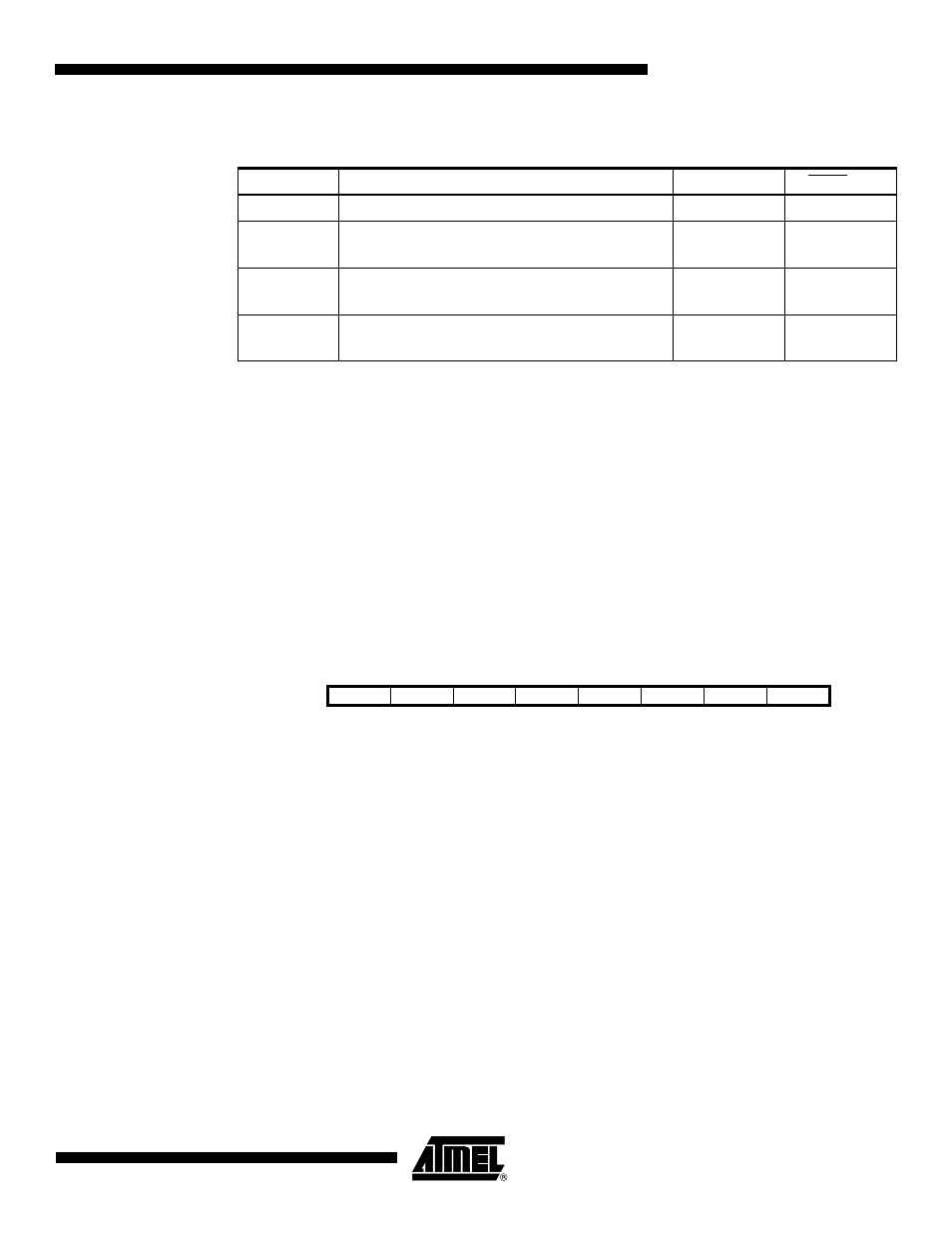
Table 16-18. Compare Output Mode, Phase and Frequency Correct PWM Mode
COM1D1..0
OCW1D Behaviour
OC1D Pin
OC1D Pin
00
Normal port operation.
Disconnected
Disconnected
01
Cleared on Compare Match when up-counting.
Set on Compare Match when down-counting.
Connected
Connected
10
Cleared on Compare Match when up-counting.
Set on Compare Match when down-counting.
Connected
Disconnected
11
Set on Compare Match when up-counting.
Cleared on Compare Match when down-counting.
Connected
Disconnected
Bit
7
6
5
4
3
2
1
0
0x26 (0x46)
FPIE1
FPEN1
FPNC1
FPES1
FPAC1
FPF1
WGM11
WGM10
TCCR1D
Read/Write
R/W
R/W
R/W
R/W
R/W
R/W
R/W
R/W
Initial value
0
0
0
0
0
0
0
0
