Usi - universal serial interface, 1 features, 2 overview – Rainbow Electronics ATtiny861_V User Manual
Page 126: Usi – universal serial interface, Data received interrupt, Wakeup from idle mode
126
2588B–AVR–11/06
ATtiny261/461/861
17. USI – Universal Serial Interface
17.1
Features
•
Two-wire Synchronous Data Transfer (Master or Slave)
•
Three-wire Synchronous Data Transfer (Master or Slave)
•
Data Received Interrupt
•
Wakeup from Idle Mode
•
In Two-wire Mode: Wake-up from All Sleep Modes, Including Power-down Mode
•
Two-wire Start Condition Detector with Interrupt Capability
17.2
Overview
The Universal Serial Interface, or USI, provides the basic hardware resources needed for serial
communication. Combined with a minimum of control software, the USI allows significantly
higher transfer rates and uses less code space than solutions based on software only. Interrupts
are included to minimize the processor load.
A simplified block diagram of the USI is shown on Figure 17-1. For the actual placement of I/O
pins, refer to
”Pinout ATtiny261/461/861” on page 2
. CPU accessible I/O Registers, including I/O
bits and I/O pins, are shown in bold. The device-specific I/O Register and bit locations are listed
in the
”Register Descriptions” on page 133
.
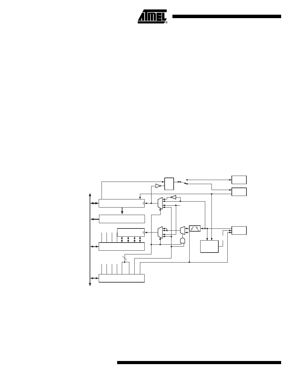
Figure 17-1. Universal Serial Interface, Block Diagram
The 8-bit USI Data Register is directly accessible via the data bus and contains the incoming
and outgoing data. The register has no buffering so the data must be read as quickly as possible
to ensure that no data is lost. The USI Data Register is a serial shift register and the most signif-
icant bit that is the output of the serial shift register is connected to one of two output pins
depending of the wire mode configuration. A transparent latch is inserted between the USI Data
Register Output and output pin, which delays the change of data output to the opposite clock
edge of the data input sampling. The serial input is always sampled from the Data Input (DI) pin
independent of the configuration.
DATA BUS
USIPF
USITC
USICLK
USICS0
USICS1
USIOIF
USIOIE
USIDC
USISIF
USIWM0
USIWM1
USISIE
Bit7
Two-wire Clock
Control Unit
DO
(Output only)
DI/SDA
(Input/Open Drain)
USCK/SCL
(Input/Open Drain)
4-bit Counter
USIDR
USISR
D Q
LE
USICR
CLOCK
HOLD
TIM0 COMP
Bit0
[1]
3
0
1
2
3
0
1
2
0
1
2
USIDB