Rainbow Electronics ATtiny861_V User Manual
Page 118
118
2588B–AVR–11/06
ATtiny261/461/861
• Bits 5,4 - COM1B1S, COM1B0S: Comparator B Output Mode, Bits 1 and 0
These bits are the shadow bits of the COM1A1 and COM1A0 bits that are described in the sec-
tion
”TCCR1A – Timer/Counter1 Control Register A” on page 113
• Bits 3,2 - COM1D1, COM1D0: Comparator D Output Mode, Bits 1 and 0
These bits control the behaviour of the Waveform Output (OCW1D) and the connection of the
Output Compare pin (OC1D). If one or both of the COM1D1:0 bits are set, the OC1D output
overrides the normal port functionality of the I/O pin it is connected to. The complementary
OC1D output is connected only in PWM modes when the COM1D1:0 bits are set to “01”. Note
that the Data Direction Register (DDR) bit corresponding to the OC1D pin must be set in order to
enable the output driver.
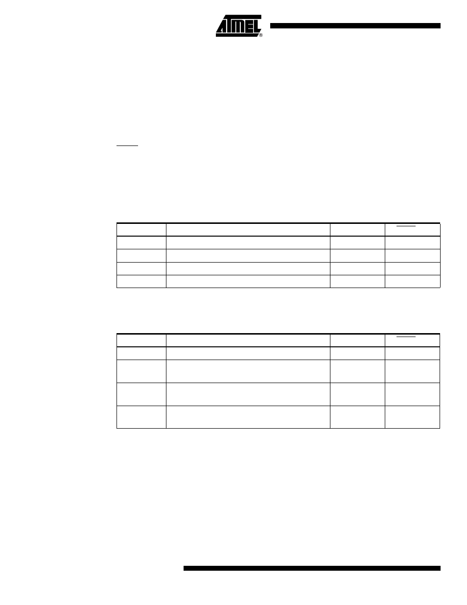
The function of the COM1D1:0 bits depends on the PWM1D and WGM10 bit settings.
Table 16-
16
shows the COM1D1:0 bit functionality when the PWM1D bit is set to a Normal Mode (non-
PWM).
Table 16-17
shows the COM1D1:0 bit functionality when the PWM1D and WGM10 bits are set
to Fast PWM Mode.
Table 16-18 on page 119
shows the COM1D1:0 bit functionality when the PWM1D and WGM10
bits are set to Phase and Frequency Correct PWM Mode.
Table 16-16. Compare Output Mode, Normal Mode (non-PWM)
COM1D1..0
OCW1D Behaviour
OC1D Pin
OC1D Pin
00
Normal port operation.
Disconnected
Disconnected
01
Toggle on Compare Match.
Connected
Disconnected
10
Clear on Compare Match.
Connected
Disconnected
11
Set on Compare Match.
Connected
Disconnected
Table 16-17. Compare Output Mode, Fast PWM Mode
COM1D1..0
OCW1D Behaviour
OC1D Pin
OC1D Pin
00
Normal port operation.
Disconnected
Disconnected
01
Cleared on Compare Match.
Set when TCNT1 = 0x000.
Connected
Connected
10
Cleared on Compare Match.
Set when TCNT1 = 0x000.
Connected
Disconnected
11
Set on Compare Match.
Clear when TCNT1 = 0x000.
Connected
Disconnected