6 compare match output unit – Rainbow Electronics ATtiny861_V User Manual
Page 99
99
2588B–AVR–11/06
ATtiny261/461/861
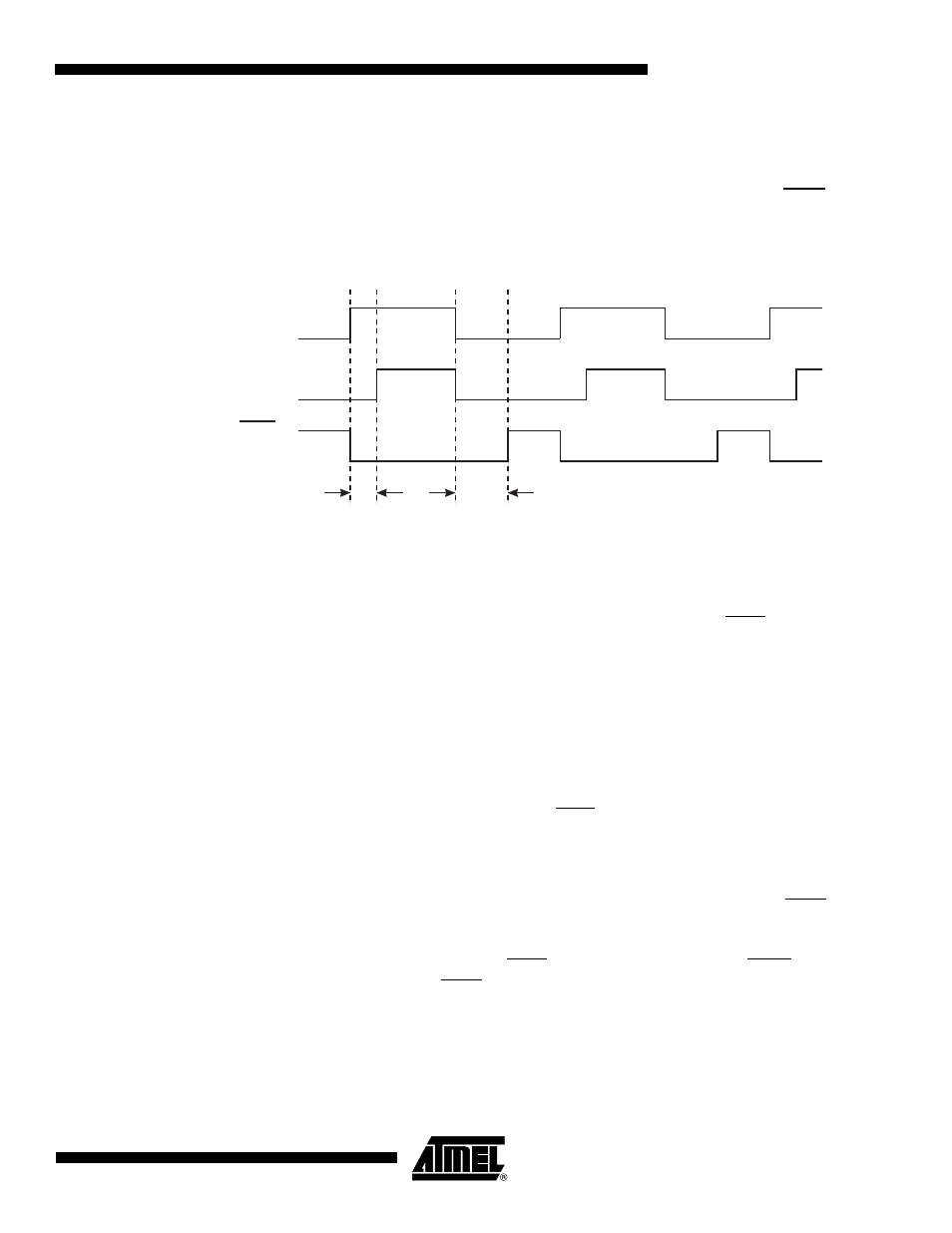
The length of the counting period is user adjustable by selecting the dead time prescaler setting
by using the DTPS11:10 control bits, and selecting then the dead time value in I/O register DT1.
The DT1 register consists of two 4-bit fields, DT1H and DT1L that control the dead time periods
of the PWM output and its' complementary output separately in terms of the number of pres-
caled dead time generator clock cycles. Thus the rising edge of OC1x and OC1x can have
different dead time periods as the t
non-overlap / rising edge
is adjusted by the 4-bit DT1H value and the
t
non-overlap / falling edge
is adjusted by the 4-bit DT1L value.
Figure 16-8. The Complementary Output Pair, COM1x1:0 = 1
16.6
Compare Match Output Unit
The Compare Output Mode (COM1x1:0) bits have two functions. The Waveform Generator uses
the COM1x1:0 bits for defining the inverted or non-inverted Waveform Output (OCW1x) at the
next Compare Match. Also, the COM1x1:0 bits control the OC1x and OC1x pin output source.
Figure 16-9
shows a simplified schematic of the logic affected by the COM1x1:0 bit setting. The
I/O Registers, I/O bits, and I/O pins in the figure are shown in bold. Only the parts of the general
I/O Port Control Registers (DDR and PORT) that are affected by the COM1x1:0 bits are shown.
In Normal Mode (non-PWM) the Dead Time Generator is disabled and it is working like a syn-
chronizer: the Output Compare (OC1x) is delayed from the Waveform Output (OCW1x) by one
timer clock cycle. Whereas in Fast PWM Mode and in Phase and Frequency Correct PWM
Mode when the COM1x1:0 bits are set to “01” both the non-inverted and the inverted Output
Compare output are generated, and an user programmable Dead Time delay is inserted for
these complementary output pairs (OC1x and OC1x). The functionality in PWM modes is similar
to Normal mode when any other COM1x1:0 bit setup is used. When referring to the OC1x state,
the reference is for the Output Compare output (OC1x) from the Dead Time Generator, not the
OC1x pin. If a system reset occur, the OC1x is reset to “0”.
The general I/O port function is overridden by the Output Compare (OC1x / OC1x) from the
Dead Time Generator if either of the COM1x1:0 bits are set. However, the OC1x pin direction
(input or output) is still controlled by the Data Direction Register (DDR) for the port pin. The Data
Direction Register bit for the OC1x and OC1x pins (DDR_OC1x and DDR_OC1x) must be set as
output before the OC1x and OC1x values are visible on the pin. The port override function is
independent of the Output Compare mode.
The design of the Output Compare Pin Configuration logic allows initialization of the OC1x state
before the output is enabled. Note that some COM1x1:0 bit settings are reserved for certain
modes of operation. For Output Compare Pin Configurations refer to
,
Table 16-3 on page 104
,
Table 16-4 on page 105
, and
Table 16-5 on page 107
.
OCnx
(COMnx = 1)
t
non-overlap / rising edge
t
non-overlap / falling edge
OCnx
OCWnx