13 tifr - timer/counter1 interrupt flag register, 14 dt1 - timer/counter1 dead time value – Rainbow Electronics ATtiny861_V User Manual
Page 124
124
2588B–AVR–11/06
ATtiny261/461/861
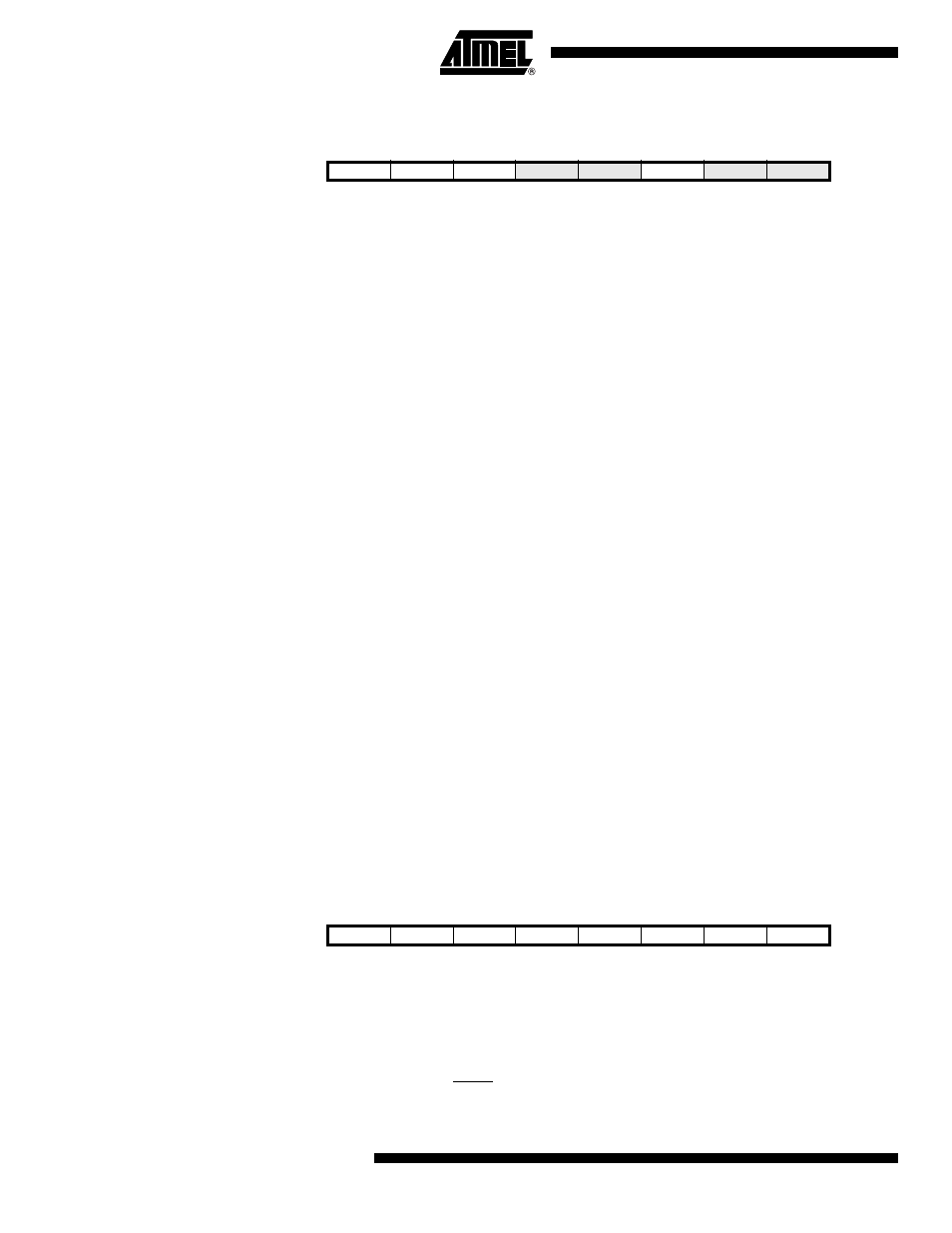
16.11.13 TIFR – Timer/Counter1 Interrupt Flag Register
• Bit 7- OCF1D: Output Compare Flag 1D
The OCF1D bit is set (one) when compare match occurs between Timer/Counter1 and the data
value in OCR1D - Output Compare Register 1D. OCF1D is cleared by hardware when executing
the corresponding interrupt handling vector. Alternatively, OCF1D is cleared, after synchroniza-
tion clock cycle, by writing a logic one to the flag. When the I-bit in SREG, OCIE1D, and OCF1D
are set (one), the Timer/Counter1 D compare match interrupt is executed.
• Bit 6 - OCF1A: Output Compare Flag 1A
The OCF1A bit is set (one) when compare match occurs between Timer/Counter1 and the data
value in OCR1A - Output Compare Register 1A. OCF1A is cleared by hardware when executing
the corresponding interrupt handling vector. Alternatively, OCF1A is cleared, after synchroniza-
tion clock cycle, by writing a logic one to the flag. When the I-bit in SREG, OCIE1A, and OCF1A
are set (one), the Timer/Counter1 A compare match interrupt is executed.
• Bit 5 - OCF1B: Output Compare Flag 1B
The OCF1B bit is set (one) when compare match occurs between Timer/Counter1 and the data
value in OCR1B - Output Compare Register 1A. OCF1B is cleared by hardware when executing
the corresponding interrupt handling vector. Alternatively, OCF1B is cleared, after synchroniza-
tion clock cycle, by writing a logic one to the flag. When the I-bit in SREG, OCIE1B, and OCF1B
are set (one), the Timer/Counter1 B compare match interrupt is executed.
• Bit 2 - TOV1: Timer/Counter1 Overflow Flag
In Normal Mode and Fast PWM Mode the TOV1 bit is set (one) each time the counter reaches
TOP at the same clock cycle when the counter is reset to BOTTOM. In Phase and Frequency
Correct PWM Mode the TOV1 bit is set (one) each time the counter reaches BOTTOM at the
same clock cycle when zero is clocked to the counter.
The bit TOV1 is cleared by hardware when executing the corresponding interrupt handling vec-
tor. Alternatively, TOV1 is cleared, after synchronization clock cycle, by writing a logical one to
the flag. When the SREG I-bit, and TOIE1 (Timer/Counter1 Overflow Interrupt Enable), and
TOV1 are set (one), the Timer/Counter1 Overflow interrupt is executed.
16.11.14 DT1 – Timer/Counter1 Dead Time Value
The dead time value register is an 8-bit read/write register.
The dead time delay of all Timer/Counter1 channels are adjusted by the dead time value regis-
ter, DT1. The register consists of two fields, DT1H3..0 and DT1L3..0, one for each
complementary output. Therefore a different dead time delay can be adjusted for the rising edge
of OC1x and the rising edge of OC1x.
Bit
7
6
5
4
3
2
1
0
0x38 (0x58)
OCF1D
OCF1A
OCF1B
OCF0A
OCF0B
TOV1
TOV0
ICF0
TIFR
Read/Write
R/W
R/W
R/W
R/W
R/W
R/W
R/W
R/W
Initial value
0
0
0
0
0
0
0
0
Bit
7
6
5
4
3
2
1
0
0x24 (0x44)
DT1H3
DT1H2
DT1H1
DT1H0
DT1L3
DT1L2
DT1L1
DT1L0
DT1
Read/Write
R/W
R/W
R/W
R/W
R/W
R/W
R/W
R/W
Initial value
0
0
0
0
0
0
0
0