4 programming time for flash when using spm, 2 register description – Rainbow Electronics ATtiny861_V User Manual
Page 166
166
2588B–AVR–11/06
ATtiny261/461/861
21.1.4
Programming Time for Flash when Using SPM
The calibrated RC Oscillator is used to time Flash accesses.
Table 21-1
shows the typical pro-
gramming time for Flash accesses from the CPU.
Note:
1. Minimum and maximum programming time is per individual operation.
21.2
Register Description
21.2.1
SPMCSR – Store Program Memory Control and Status Register
The Store Program Memory Control and Status Register contains the control bits needed to con-
trol the Program memory operations.
• Bits 7:5 – Res: Reserved Bits
These bits are reserved bits in the ATtiny261/461/861 and always read as zero.
• Bit 4 – CTPB: Clear Temporary Page Buffer
If the CTPB bit is written while filling the temporary page buffer, the temporary page buffer will be
cleared and the data will be lost.
• Bit 3 – RFLB: Read Fuse and Lock Bits
An LPM instruction within three cycles after RFLB and SPMEN are set in the SPMCSR Register,
will read either the Lock bits or the Fuse bits (depending on Z0 in the Z-pointer) into the destina-
tion register. See
”EEPROM Write Prevents Writing to SPMCSR” on page 164
for details.
• Bit 2 – PGWRT: Page Write
If this bit is written to one at the same time as SPMEN, the next SPM instruction within four clock
cycles executes Page Write, with the data stored in the temporary buffer. The page address is
taken from the high part of the Z-pointer. The data in R1 and R0 are ignored. The PGWRT bit
will auto-clear upon completion of a Page Write, or if no SPM instruction is executed within four
clock cycles. The CPU is halted during the entire Page Write operation.
• Bit 1 – PGERS: Page Erase
If this bit is written to one at the same time as SPMEN, the next SPM instruction within four clock
cycles executes Page Erase. The page address is taken from the high part of the Z-pointer. The
data in R1 and R0 are ignored. The PGERS bit will auto-clear upon completion of a Page Erase,
or if no SPM instruction is executed within four clock cycles. The CPU is halted during the entire
Page Write operation.
Table 21-1.
Symbol
Min Programming Time
Max Programming Time
Flash write (Page Erase, Page Write, and
write Lock bits by SPM)
3.7 ms
4.5 ms
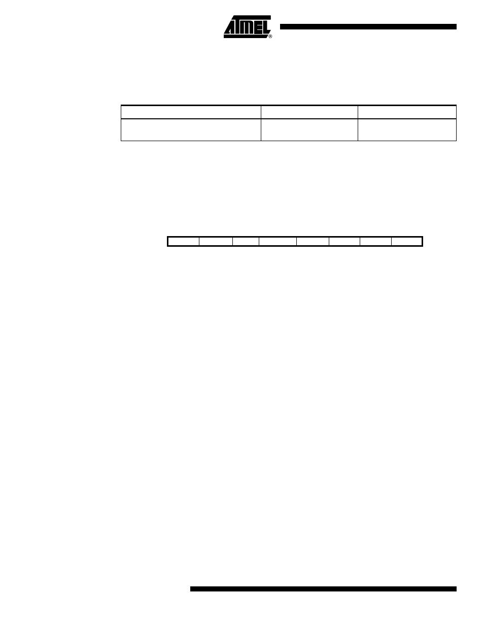
Bit
7
6
5
4
3
2
1
0
0x37 (0x57)
–
–
–
CTPB
RFLB
PGWRT
PGERS
SPMEN
SPMCSR
Read/Write
R
R
R
R/W
R/W
R/W
R/W
R/W
Initial Value
0
0
0
0
0
0
0
0