6 changing channel or reference selection – Rainbow Electronics ATtiny861_V User Manual
Page 147
147
2588B–AVR–11/06
ATtiny261/461/861
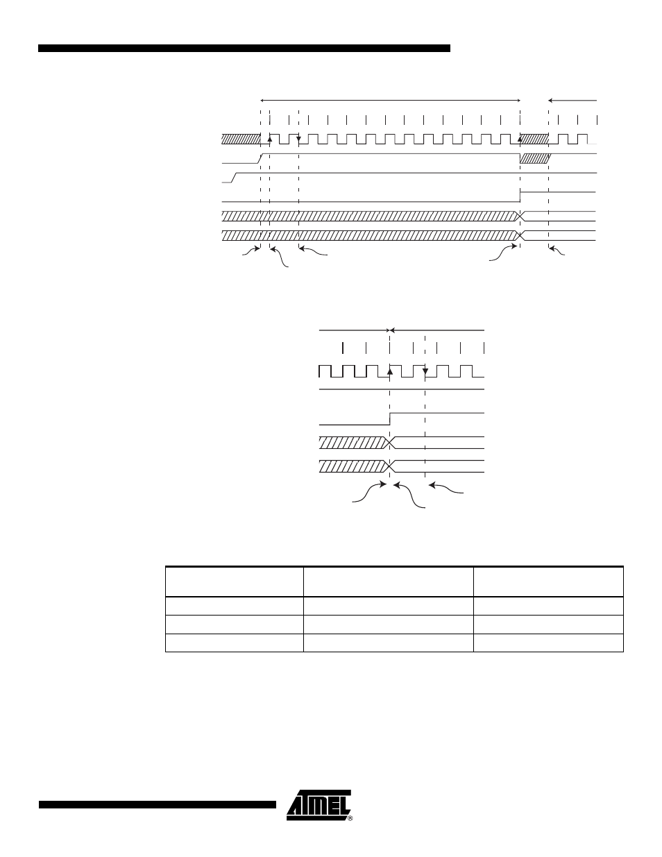
Figure 19-6. ADC Timing Diagram, Auto Triggered Conversion
Figure 19-7. ADC Timing Diagram, Free Running Conversion
19.6
Changing Channel or Reference Selection
The MUX5:0 and REFS2:0 bits in the ADMUX Register are single buffered through a temporary
register to which the CPU has random access. This ensures that the channels and reference
selection only takes place at a safe point during the conversion. The channel and reference
selection is continuously updated until a conversion is started. Once the conversion starts, the
channel and reference selection is locked to ensure a sufficient sampling time for the ADC. Con-
tinuous updating resumes in the last ADC clock cycle before the conversion completes (ADIF in
Table 19-1.
ADC Conversion Time
Condition
Sample & Hold
(Cycles from Start of Conversion)
Conversion Time (Cycles)
First conversion
13.5
25
Normal conversions
1.5
13
Auto Triggered conversions
2
13.5
1
2
3
4
5
6
7
8
9
10
11
12
13
Sign and MSB of Result
LSB of Result
ADC Clock
Trigger
Source
ADIF
ADCH
ADCL
Cycle Number
1
2
One Conversion
Next Conversion
Conversion
Complete
Prescaler
Reset
ADATE
Prescaler
Reset
Sample &
Hold
MUX and REFS
Update
11
12
13
Sign and MSB of Result
LSB of Result
ADC Clock
ADSC
ADIF
ADCH
ADCL
Cycle Number
1
2
One Conversion
Next Conversion
3
4
Conversion
Complete
Sample & Hold
MUX and REFS
Update