1 alternate functions of port b – Rainbow Electronics ATtiny861_V User Manual
Page 61
61
2588B–AVR–11/06
ATtiny261/461/861
12.3.1
Alternate Functions of Port B
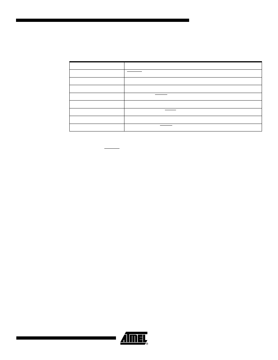
The Port B pins with alternate function are shown in
Table 12-3
.
The alternate pin configuration is as follows:
• Port B, Bit 7 - RESET/ dW/ ADC10/ PCINT15
RESET, Reset pin: When the RSTDISBL Fuse is programmed, this pin functions as a normal I/O
pin, and the part will have to rely on Power-on Reset and Brown-out Reset as its reset sources.
When the RSTDISBL Fuse is unprogrammed, the reset circuitry is connected to the pin, and the
pin can not be used as an I/O pin.
If PB7 is used as a reset pin, DDB7, PORTB7 and PINB7 will all read 0.
dW: When the debugWIRE Enable (DWEN) Fuse is programmed and Lock bits are unpro-
grammed, the RESET port pin is configured as a wire-AND (open-drain) bi-directional I/O pin
with pull-up enabled and becomes the communication gateway between target and emulator.
ADC10: ADC input Channel 10. Note that ADC input channel 10 uses analog power.
PCINT15: Pin Change Interrupt source 15.
• Port B, Bit 6 - ADC9/ T0/ INT0/ PCINT14
ADC9: ADC input Channel 9. Note that ADC input channel 9 uses analog power.
T0: Timer/Counter0 counter source.
INT0: The PB6 pin can serve as an External Interrupt source 0.
PCINT14: Pin Change Interrupt source 14.
• Port B, Bit 5 - XTAL2/ CLKO/ ADC8/ PCINT13
XTAL2: Chip clock Oscillator pin 2. Used as clock pin for crystal Oscillator or Low-frequency
crystal Oscillator. When used as a clock pin, the pin can not be used as an I/O pin.
CLKO: The divided system clock can be output on the PB5 pin, if the CKOUT Fuse is pro-
grammed, regardless of the PORTB5 and DDB5 settings. It will also be output during reset.
OC1D Output Compare Match output: The PB5 pin can serve as an external output for the
Timer/Counter1 Compare Match D when configured as an output (DDA1 set). The OC1D pin is
also the output pin for the PWM mode timer function.
Table 12-3.
Port B Pins Alternate Functions
Port Pin
Alternate Function
PB7
RESET / dW / ADC10 / PCINT15
PB6
ADC9 / T0 / INT0 / PCINT14
PB5
XTAL2 / CLKO / OC1D / ADC8 / PCINT13
PB4
XTAL1 / CLKI / OC1D / ADC7 / PCINT12
PB3
OC1B / PCINT11
PB2
SCK / USCK / SCL / OC1B /PCINT10
PB1
MISO / DO / OC1A / PCINT9
PB0
MOSI / DI / SDA / OC1A / PCINT8