8 register description, 1 mcucr - mcu control register, 2 prr - power reduction register – Rainbow Electronics ATtiny861_V User Manual
Page 37
37
2588B–AVR–11/06
ATtiny261/461/861
Refer to
”DIDR0 – Digital Input Disable Register 0” on page 160
for details.
8.8
Register Description
8.8.1
MCUCR – MCU Control Register
The MCU Control Register contains control bits for power management.
• Bit 5 – SE: Sleep Enable
The SE bit must be written to logic one to make the MCU enter the sleep mode when the SLEEP
instruction is executed. To avoid the MCU entering the sleep mode unless it is the programmer’s
purpose, it is recommended to write the Sleep Enable (SE) bit to one just before the execution of
the SLEEP instruction and to clear it immediately after waking up.
• Bits 4, 3 – SM1:0: Sleep Mode Select Bits 2..0
These bits select between the three available sleep modes as shown in
Table 8-2
.
• Bit 2 – Res: Reserved Bit
This bit is a reserv ed bit in the ATtiny261/461/861 and will always read as zero.
8.8.2
PRR – Power Reduction Register
• Bits 7, 6, 5, 4- Res: Reserved Bits
These bits are reserved bits in the ATtiny261/461/861 and will always read as zero.
• Bit 3- PRTIM1: Power Reduction Timer/Counter1
Writing a logic one to this bit shuts down the Timer/Counter1 module. When the Timer/Counter1
is enabled, operation will continue like before the shutdown.
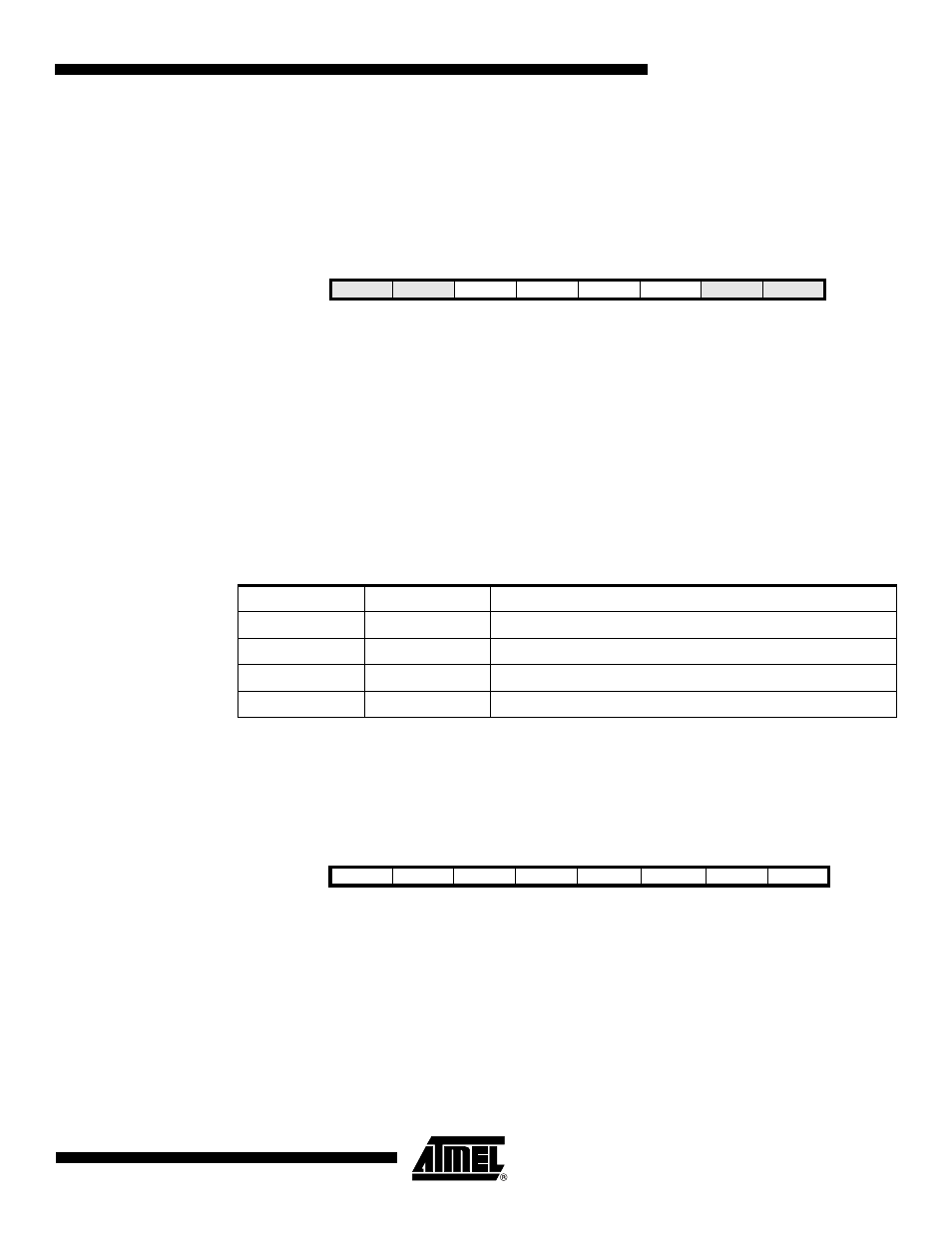
Bit
7
6
5
4
3
2
1
0
0x35 (0x55)
–
PUD
SE
SM1
SM0
—
ISC01
ISC00
MCUCR
Read/Write
R
R/W
R/W
R/W
R/W
R
R/W
R/W
Initial Value
0
0
0
0
0
0
0
0
Table 8-2.
Sleep Mode Select
SM1
SM0
Sleep Mode
0
0
Idle
0
1
ADC Noise Reduction
1
0
Power-down
1
1
Standby
Bit
7
6
5
4
3
2
1
0
0x36 (0x56)
–
-
-
-
PRTIM1
PRTIM0
PRUSI
PRADC
PRR
Read/Write
R
R
R
R
R/W
R/W
R/W
R/W
Initial Value
0
0
0
0
0
0
0
0