Rainbow Electronics ATmega64C1 User Manual
Page 69
69
7647A–AVR–02/08
ATmega32/64/M1/C1
MISO, Master Data input, Slave Data output pin for SPI channel. When the SPI is enabled as a
master, this pin is configured as an input regardless of the setting of DDB0. When the SPI is
enabled as a slave, the data direction of this pin is controlled by DDB0. When the pin is forced to
be an input, the pull-up can still be controlled by the PORTB0 and PUD bits.
PSCOUT2A, Output 2A of PSC.
PCINT0, Pin Change Interrupt 0.
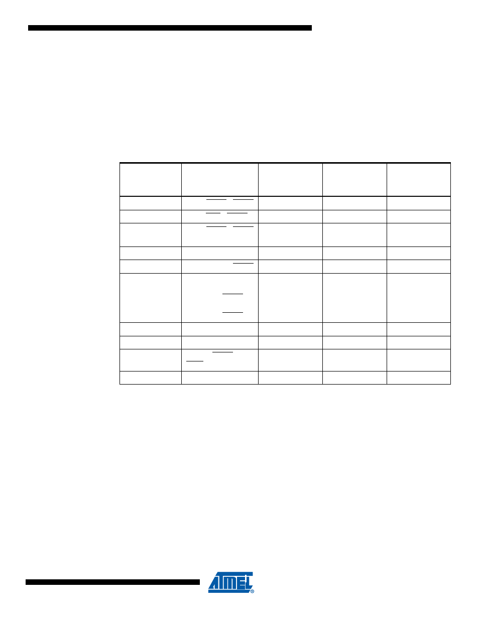
and
relates the alternate functions of Port B to the overriding signals shown
in
.
Table 9-4.
Overriding Signals for Alternate Functions in PB7..PB4
Signal Name
PB7/ADC4/
PSCOUT0B/SCK/
PCINT7
PB6/ADC7/
PSCOUT1B/
PCINT6
PB5/ADC6/
INT2/ACMPN1/
AMP2-/PCINT5
PB4/AMP0+/
PCINT4
PUOE
SPE • MSTR • SPIPS
0
0
0
PUOV
PB7 • PUD • SPIPS
0
0
0
DDOE
SPE • MSTR • SPIPS
+ PSCen01
PSCen11
0
0
DDOV
PSCen01
1
0
0
PVOE
SPE • MSTR • SPIPS
PSCen11
0
0
PVOV
PSCout01 • SPIPS +
PSCout01 •
PSCen01 • SPIPS
+ PSCout01 •
PSCen01 • SPIPS
PSCOUT11
0
0
DIEOE
ADC4D
ADC7D
ADC6D + In2en
AMP0ND
DIEOV
0
0
In2en
0
DI
SCKin • SPIPS •
ireset
ICP1B
INT2
AIO
ADC4
ADC7
ADC6
AMP0+