2 the eeprom address registers - eearh and eearl, 3 the eeprom data register - eedr, 4 the eeprom control register - eecr – Rainbow Electronics ATmega64C1 User Manual
Page 23
23
7647A–AVR–02/08
ATmega32/64/M1/C1
4.3.2
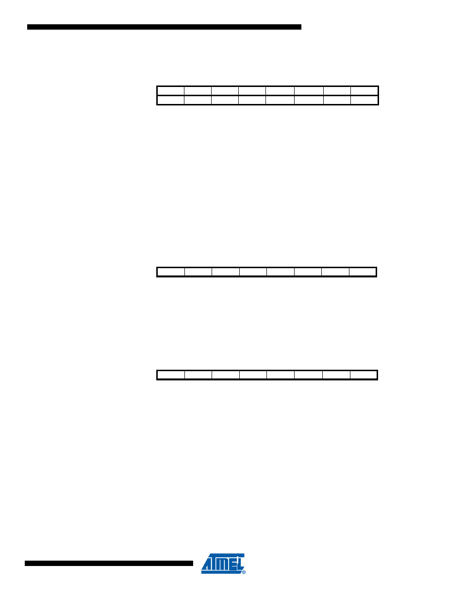
The EEPROM Address Registers – EEARH and EEARL
• Bits 15.10 – Reserved Bits
These bits are reserved bits in the ATmega32/64/M1/C1 and will always read as zero.
• Bits 9..0 – EEAR8..0: EEPROM Address
The EEPROM Address Registers – EEARH and EEARL specify the EEPROM address in the
1024/2048 bytes EEPROM space. The EEPROM data bytes are addressed linearly between 0
and 1023. The initial value of EEAR is undefined. A proper value must be written before the
EEPROM may be accessed.
4.3.3
The EEPROM Data Register – EEDR
• Bits 7..0 – EEDR7.0: EEPROM Data
For the EEPROM write operation, the EEDR Register contains the data to be written to the
EEPROM in the address given by the EEAR Register. For the EEPROM read operation, the
EEDR contains the data read out from the EEPROM at the address given by EEAR.
4.3.4
The EEPROM Control Register – EECR
• Bits 7..6 – Reserved Bits
These bits are reserved bits in the ATmega32/64/M1/C1 and will always read as zero.
• Bits 5..4 – EEPM1 and EEPM0: EEPROM Programming Mode Bits
The EEPROM Programming mode bit setting defines which programming action that will be trig-
gered when writing EEWE. It is possible to program data in one atomic operation (erase the old
value and program the new value) or to split the Erase and Write operations in two different
operations. The Programming times for the different modes are shown in
Bit
15
14
13
12
11
10
9
8
–
–
–
–
–
-
EEAR9
EEAR8
EEARH
EEAR7
EEAR6
EEAR5
EEAR4
EEAR3
EEAR2
EEAR1
EEAR0
EEARL
7
6
5
4
3
2
1
0
Read/Write
R
R
R
R
R
R/W
R/W
R/W
R/W
R/W
R/W
R/W
R/W
R/W
R/W
R/W
Initial Value
0
0
0
0
0
0
0
X
X
X
X
X
X
X
X
X
Bit
7
6
5
4
3
2
1
0
EEDR7
EEDR6
EEDR5
EEDR4
EEDR3
EEDR2
EEDR1
EEDR0
EEDR
Read/Write
R/W
R/W
R/W
R/W
R/W
R/W
R/W
R/W
Initial Value
0
0
0
0
0
0
0
0
Bit
7
6
5
4
3
2
1
0
–
–
EEPM1
EEPM0
EERIE
EEMWE
EEWE
EERE
EECR
Read/Write
R
R
R/W
R/W
R/W
R/W
R/W
R/W
Initial Value
0
0
X
X
0
0
X
0