6 stack pointer, 7 instruction execution timing, Ed in – Rainbow Electronics ATmega64C1 User Manual
Page 16: Figure 3-3
16
7647A–AVR–02/08
ATmega32/64/M1/C1
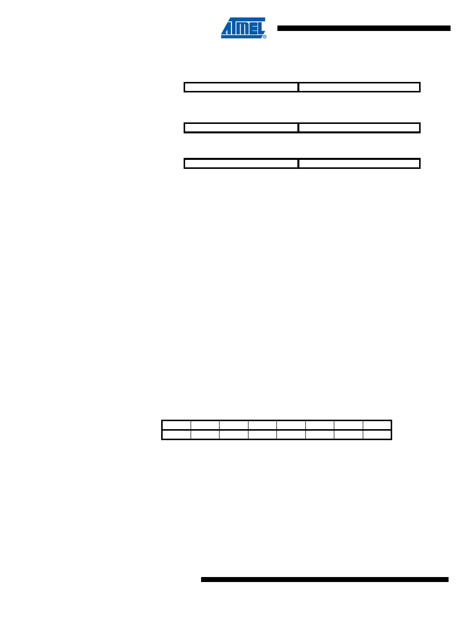
Figure 3-3.
The X-, Y-, and Z-registers
In the different addressing modes these address registers have functions as fixed displacement,
automatic increment, and automatic decrement (see the instruction set reference for details).
3.6
Stack Pointer
The Stack is mainly used for storing temporary data, for storing local variables and for storing
return addresses after interrupts and subroutine calls. The Stack Pointer Register always points
to the top of the Stack. Note that the Stack is implemented as growing from higher memory loca-
tions to lower memory locations. This implies that a Stack PUSH command decreases the Stack
Pointer.
The Stack Pointer points to the data SRAM Stack area where the Subroutine and Interrupt
Stacks are located. This Stack space in the data SRAM must be defined by the program before
any subroutine calls are executed or interrupts are enabled. The Stack Pointer must be set to
point above 0x100. The Stack Pointer is decremented by one when data is pushed onto the
Stack with the PUSH instruction, and it is decremented by two when the return address is
pushed onto the Stack with subroutine call or interrupt. The Stack Pointer is incremented by one
when data is popped from the Stack with the POP instruction, and it is incremented by two when
data is popped from the Stack with return from subroutine RET or return from interrupt RETI.
The AVR Stack Pointer is implemented as two 8-bit registers in the I/O space. The number of
bits actually used is implementation dependent. Note that the data space in some implementa-
tions of the AVR architecture is so small that only SPL is needed. In this case, the SPH Register
will not be present.
3.7
Instruction Execution Timing
This section describes the general access timing concepts for instruction execution. The AVR
CPU is driven by the CPU clock clk
CPU
, directly generated from the selected clock source for the
chip. No internal clock division is used.
15
XH
XL
0
X-register
7
0
7
0
R27 (0x1B)
R26 (0x1A)
15
YH
YL
0
Y-register
7
0
7
0
R29 (0x1D)
R28 (0x1C)
15
ZH
ZL
0
Z-register
7
0
7
0
R31 (0x1F)
R30 (0x1E)
Bit
15
14
13
12
11
10
9
8
SP15
SP14
SP13
SP12
SP11
SP10
SP9
SP8
SPH
SP7
SP6
SP5
SP4
SP3
SP2
SP1
SP0
SPL
7
6
5
4
3
2
1
0
Read/Write
R/W
R/W
R/W
R/W
R/W
R/W
R/W
R/W
R/W
R/W
R/W
R/W
R/W
R/W
R/W
R/W
Initial Value
0
0
0
0
0
0
0
0
0
0
0
0
0
0
0
0